
The semiconductor industry is entering a new phase in which traditional transistor scaling alone is no longer sufficient to deliver the performance, bandwidth, power efficiency, and integration density demanded by artificial intelligence (AI), high-performance computing (HPC), advanced memory, and next-generation electronics. As a result, semiconductor manufacturers are increasingly turning to advanced packaging and 3D integration technologies, creating strong momentum for hybrid bonding.
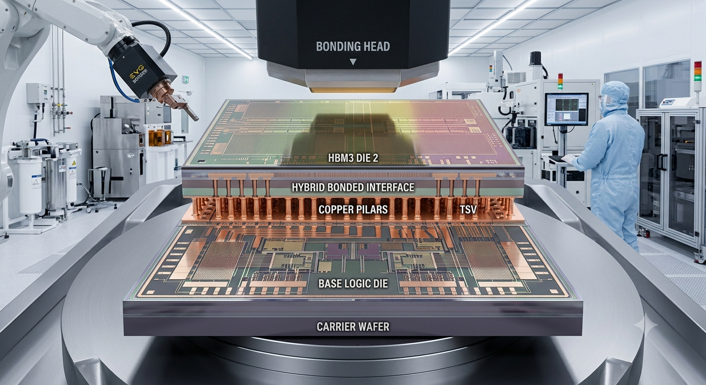
Hybrid bonding enables direct connections between semiconductor wafers or dies by combining dielectric bonding with copper-to-copper interconnects. Unlike conventional solder-based approaches, the technology supports extremely fine-pitch interconnections, making it well suited to chiplet architectures, stacked memory, 3D integrated circuits, and heterogeneous integration.
According to MarketsandMarkets, the global Hybrid Bonding Market is projected to grow from USD 164.7 million in 2025 to USD 633.9 million by 2032, registering a 21.2% CAGR during the forecast period.
Hybrid Bonding Becomes a Critical Advanced Packaging Technology
Hybrid bonding is emerging as an important technology for addressing the limitations of conventional semiconductor interconnects. It creates direct electrical and mechanical connections between wafers or dies, allowing manufacturers to achieve higher interconnect density while reducing signal latency and power consumption.
The technology can be applied across several packaging architectures, including:
- Wafer-to-Wafer (W2W)
- Die-to-Wafer (D2W)
- Die-to-Die (D2D)
Hybrid bonding also supports 2.5D packaging, 3D stacked ICs, and heterogeneous integration, providing semiconductor manufacturers with greater flexibility in combining different chips and functional blocks within a single package.
AI and HPC Accelerate Hybrid Bonding Demand
The rapid growth of AI infrastructure is one of the strongest factors supporting hybrid bonding adoption.
AI accelerators, GPUs, high-performance processors, and memory systems must process enormous amounts of data while maintaining high bandwidth and controlling power consumption. Conventional packaging approaches can become increasingly challenging as designers seek higher interconnect densities and shorter communication paths between processing and memory components.
Hybrid bonding addresses these requirements by enabling dense vertical interconnections between semiconductor layers. This makes it particularly attractive for AI accelerators, HPC processors, advanced logic, and memory applications. MarketsandMarkets expects computing and logic applications to grow at a 26.0% CAGR from 2025 to 2032, highlighting the importance of these applications to market expansion.
Download PDF Brochure @ https://www.marketsandmarkets.com/pdfdownloadNew.asp?id=2641237
Chiplets Reshape Semiconductor Design
The growing adoption of chiplet architectures is another major opportunity for hybrid bonding.
Instead of manufacturing an entire complex processor as one large die, chiplet-based designs divide functionality into smaller dies that can be integrated within a single package. This approach can improve design flexibility, manufacturing efficiency, and scalability.
However, chiplets require extremely dense and reliable connections between individual dies. Hybrid bonding can provide the fine-pitch interconnects needed to connect these components efficiently.
The growing use of chiplets in AI, HPC, and advanced logic devices is therefore accelerating demand for die-to-die hybrid bonding. MarketsandMarkets projects the die-to-die segment to register a 35.3% CAGR from 2025 to 2032, making it one of the fastest-growing areas of the market.
High-Bandwidth Memory Creates New Growth Opportunities
High-bandwidth memory (HBM) has become increasingly important for AI and high-performance computing systems. HBM uses vertically stacked memory dies to provide high data-transfer rates within a compact footprint.
As AI workloads grow, demand for memory bandwidth continues to increase. Hybrid bonding can support dense vertical interconnections in advanced memory architectures, creating opportunities for its adoption in next-generation HBM and stacked-memory solutions.
MarketsandMarkets identifies HBM and memory stacking as important growth areas for hybrid bonding, alongside AI processors and advanced logic devices.
3D Integration Drives the Next Wave of Packaging
Traditional semiconductor scaling has delivered significant performance improvements for decades. However, increasing physical and economic challenges associated with continued miniaturization are encouraging chipmakers to explore 3D integration.
3D integration allows semiconductor components to be stacked vertically rather than relying solely on two-dimensional scaling. Hybrid bonding is particularly valuable in these architectures because it enables extremely dense vertical connections.
This approach can help improve:
- Bandwidth
- Latency
- Power efficiency
- Integration density
- Form-factor efficiency
- System-level performance
The shift toward 3D stacked ICs and heterogeneous integration is therefore expected to remain a major catalyst for the Hybrid Bonding Market.
Copper-to-Copper Bonding Gains Momentum
By bonding type, copper-to-copper (Cu-Cu) technology is expected to lead the market and register strong growth during the forecast period.
Cu-Cu hybrid bonding provides a direct electrical connection between copper interconnects while eliminating the need for conventional microbumps. This allows semiconductor manufacturers to achieve much finer pitches and higher interconnect density.
The combination of fine-pitch connectivity, improved electrical performance, and reduced interconnect dimensions makes Cu-Cu bonding increasingly attractive for advanced logic, memory, and 3D integration applications.
Wafer Bonders Remain Central to Manufacturing
The equipment ecosystem surrounding hybrid bonding includes:
- Wafer bonders
- Surface preparation tools
- Inspection and metrology tools
- Cleaning and CMP systems
The wafer bonders segment is expected to exhibit the highest CAGR during the forecast period. Wafer-to-wafer bonding requires extremely accurate alignment, clean surfaces, and controlled process conditions.
As semiconductor manufacturers scale production of stacked memory, CIS, and 3D logic devices, demand for high-precision wafer bonding equipment is expected to increase.
Surface Preparation and Metrology Become More Important
Hybrid bonding requires exceptionally clean and precisely prepared surfaces. Even small particles or imperfections can affect bonding quality and manufacturing yield.
This makes surface preparation, cleaning, CMP, inspection, and metrology critical components of the hybrid bonding manufacturing ecosystem.
As manufacturers move toward smaller interconnect pitches, process control becomes increasingly demanding. Equipment suppliers that can improve alignment accuracy, surface quality, contamination control, and defect detection will play an important role in enabling high-volume production.
Heterogeneous Integration Opens New Opportunities
Heterogeneous integration combines different semiconductor components, technologies, materials, or process nodes within a single package.
This approach is becoming increasingly important as semiconductor designers seek to combine:
- Logic
- Memory
- Analog
- RF
- Accelerators
- Sensors
- Other specialized processing components
MarketsandMarkets expects the heterogeneous integration segment to register the fastest growth during the forecast period. Hybrid bonding is well positioned to support this transition because of its ability to provide high-density connections between multiple dies.
Semiconductor Investment Supports Market Expansion
The increasing investment by semiconductor foundries and integrated device manufacturers (IDMs) in advanced packaging capacity is strengthening the hybrid bonding ecosystem.
Leading manufacturers are expanding their capabilities in:
- 3D integration
- Advanced memory packaging
- Chiplets
- Heterogeneous integration
- Wafer-level packaging
- High-density interconnects
At the same time, equipment manufacturers are developing solutions capable of delivering higher throughput, improved alignment accuracy, and better process control.
These developments are helping hybrid bonding transition from specialized applications toward broader high-volume manufacturing.
Asia Pacific Leads the Market
Asia Pacific is a critical region for the Hybrid Bonding Market because it contains a significant concentration of semiconductor foundries, memory manufacturers, equipment suppliers, and electronics manufacturing capabilities.
According to MarketsandMarkets, Asia Pacific accounted for 51.6% of hybrid bonding market revenue in 2024. The region benefits from strong semiconductor manufacturing infrastructure and continued investments in advanced packaging.
Countries including Taiwan, South Korea, China, and Japan are important contributors to the region’s semiconductor ecosystem.
China is also expected to hold a significant share of the global market in 2025, supported by semiconductor manufacturing expansion, advanced packaging investments, and efforts to strengthen domestic semiconductor capabilities.
Key Challenges
Despite its strong growth prospects, hybrid bonding faces several technical and commercial challenges.
Manufacturing Complexity
Hybrid bonding requires extremely precise alignment and surface preparation. Maintaining consistent performance at high production volumes can be difficult.
Yield Management
As interconnect dimensions become smaller, defects and particles can have a greater impact on yield. Manufacturers therefore need advanced inspection and metrology capabilities.
High Equipment Costs
Advanced bonding equipment, cleaning systems, metrology tools, and surface-preparation technologies require significant capital investment.
Process Integration
Hybrid bonding must be integrated with existing semiconductor manufacturing and packaging processes. Developing optimized workflows can require substantial engineering and qualification efforts.
Skilled Workforce
The complexity of hybrid bonding manufacturing creates demand for engineers and technicians with expertise in semiconductor packaging, materials science, equipment engineering, and process control.
Competitive Landscape
The Hybrid Bonding Market includes semiconductor equipment and advanced packaging technology providers such as EV Group (EVG), Applied Materials, SUSS MicroTec, BE Semiconductor Industries (Besi), Kulicke & Soffa, Tokyo Electron, ASMPT, Lam Research, Onto Innovation, DISCO, KLA, and others.
Competition is increasingly centered on improving:
- Bonding accuracy
- Throughput
- Yield
- Surface preparation
- Metrology
- Process automation
- High-volume manufacturing capabilities
Strategic collaborations between equipment suppliers, semiconductor manufacturers, foundries, and packaging companies are also becoming increasingly important as the technology moves toward broader commercial adoption.
Future Outlook
The Hybrid Bonding Market is positioned for substantial growth as semiconductor manufacturers move beyond conventional scaling and embrace advanced packaging.
From AI accelerators and HBM to chiplets, 3D stacked ICs, and heterogeneous integration, the technology is becoming an important enabler of next-generation semiconductor architectures.
The global hybrid bonding market is projected to reach USD 633.9 million by 2032 from USD 164.7 million in 2025, registering a CAGR of 21.2% from 2025 to 2032., hybrid bonding is moving from a specialized packaging technique toward a strategic component of semiconductor manufacturing.
The next phase of growth will depend on improvements in bonding precision, equipment throughput, process automation, yield optimization, and manufacturing scalability.
As the semiconductor industry enters an era defined by AI, 3D integration, chiplets, and heterogeneous architectures, hybrid bonding is poised to become one of the technologies shaping the future of advanced packaging.
FAQs:
1. What is the current size of the Hybrid Bonding Market?
The global Hybrid Bonding Market is projected to grow from USD 164.7 million in 2025 to USD 633.9 million by 2032, representing a CAGR of 21.2% during the forecast period.
2. What is driving the growth of the Hybrid Bonding Market?
Growth is primarily driven by the increasing adoption of 3D semiconductor integration, AI accelerators, high-bandwidth memory (HBM), chiplet architectures, and heterogeneous integration. The need for higher bandwidth, lower latency, improved power efficiency, and finer interconnect density is encouraging semiconductor manufacturers to adopt hybrid bonding.
3. Which segment is expected to grow fastest in the Hybrid Bonding Market?
The die-to-die (D2D) packaging architecture is projected to register a 35.3% CAGR from 2025 to 2032. The growth is linked to increasing adoption of chiplet-based designs and heterogeneous integration for AI, HPC, and advanced logic applications.
4. What are the major applications of hybrid bonding?
Major applications include AI and high-performance computing, advanced memory and HBM, 3D stacked ICs, image sensors, advanced logic, mobile processors, and heterogeneous semiconductor integration.