
The semiconductor industry is undergoing a major transformation as demand for advanced chips, high-performance computing, artificial intelligence (AI), electric vehicles, and connected devices continues to increase. Semiconductor manufacturers are investing in advanced fabrication facilities to improve production efficiency, enhance wafer quality, reduce operational costs, and support increasingly complex chip designs. In this evolving landscape, automation has become a critical component of modern semiconductor manufacturing.
The Fab Automation Industry Report highlights how technologies such as Automated Material Handling Systems (AMHS), industrial robotics, Manufacturing Execution Systems (MES), and advanced process control solutions are reshaping semiconductor fabrication facilities. These technologies enable manufacturers to automate material movement, improve production visibility, minimize human intervention, and maintain consistent manufacturing quality. The fab automation market is expected to grow from USD 25.24 billion in 2025 to USD 41.44 billion by 2032, growing at a CAGR of 7.3%.
As semiconductor fabrication processes become more sophisticated, traditional manufacturing approaches are increasingly challenged by the need for precision, speed, and operational flexibility. Automation solutions help semiconductor fabs manage complex production workflows while supporting higher throughput and improved equipment utilization.
According to the market landscape covered by MarketsandMarkets, the growing adoption of automation technologies across semiconductor fabrication facilities is creating significant opportunities for technology providers, equipment manufacturers, and software developers.
Growing Demand for Automation in Semiconductor Manufacturing
The increasing complexity of semiconductor devices is one of the primary factors driving the adoption of fab automation technologies. Advanced semiconductor nodes require highly controlled manufacturing environments, precise process execution, and strict contamination management. Even minor production errors can affect wafer quality and increase manufacturing costs.
Automation enables semiconductor manufacturers to standardize repetitive operations and maintain consistent production conditions. Automated systems can perform material transportation, wafer handling, equipment monitoring, and production scheduling with greater accuracy and reliability.
The expansion of semiconductor manufacturing capacity across major markets is also strengthening demand for automated fabrication facilities. Governments and private companies are investing in domestic semiconductor production to improve supply chain resilience and reduce dependence on external manufacturing ecosystems.
Additionally, the growing adoption of AI chips, memory devices, processors, and advanced packaging technologies is increasing pressure on semiconductor manufacturers to improve productivity. The Fab Automation Industry Report reflects the growing importance of integrated automation solutions in supporting these manufacturing requirements.
Download PDF Brochure @ https://www.marketsandmarkets.com/pdfdownloadNew.asp?id=219676619
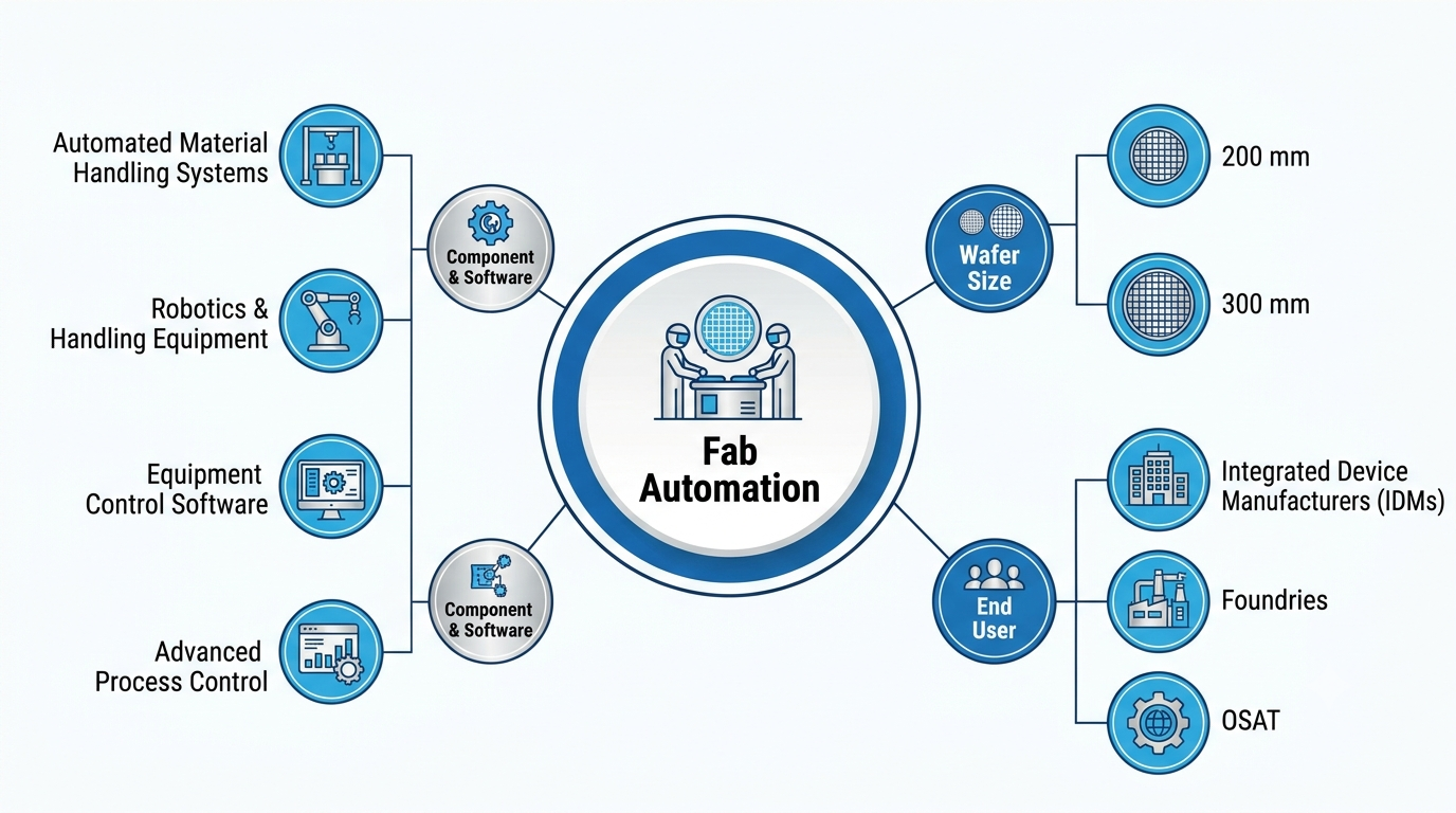
AMHS Transforming Material Movement Across Semiconductor Fabs
Automated Material Handling Systems (AMHS) represent one of the most important technologies in semiconductor fab automation. These systems automate the transportation, storage, and delivery of semiconductor wafers and other materials throughout fabrication facilities.
Semiconductor manufacturing involves hundreds of complex processing steps, with wafers moving between different production equipment and manufacturing areas. Manual transportation can increase processing delays, contamination risks, and operational inefficiencies.
AMHS addresses these challenges through automated transport technologies, including overhead hoist transport systems, automated guided vehicles, stockers, conveyors, and robotic material handling equipment.
Modern AMHS solutions provide several operational advantages:
-
Improved Material Transportation: Automated systems move wafer carriers between manufacturing equipment with minimal human intervention.
-
Reduced Contamination Risks: Automated handling reduces direct human contact with sensitive semiconductor materials.
-
Higher Production Efficiency: Intelligent transportation systems minimize material movement delays and improve equipment utilization.
-
Real-Time Tracking: Advanced software provides visibility into material locations and transportation status.
-
Optimized Workflow Management: Automated scheduling helps coordinate material movement across multiple production areas.
The integration of AI and machine learning into AMHS is further improving transportation efficiency. Predictive algorithms can analyze production requirements, identify potential bottlenecks, and optimize material delivery routes.
As semiconductor fabs become larger and more complex, AMHS will remain a fundamental part of next-generation manufacturing infrastructure.
Robotics and Wafer Handling Equipment Enhancing Manufacturing Precision
Robotics is another major pillar of the Fab Automation Industry Report, supporting the transition toward highly automated semiconductor production environments. Semiconductor fabrication requires precise wafer positioning, controlled material transfers, and reliable equipment operation. Robotics helps manufacturers perform these activities while reducing the possibility of human errors and material contamination.
Advanced semiconductor fabs use different types of robots, including atmospheric wafer-handling robots, vacuum robots, cleanroom robots, industrial robots, and automated inspection systems. These robots are integrated into manufacturing equipment to support wafer loading, unloading, transportation, and positioning.
The growing adoption of advanced semiconductor nodes is increasing the importance of robotic automation. Manufacturing processes involving extreme ultraviolet (EUV) lithography, deposition, etching, and inspection require accurate wafer handling and stable operating conditions.
Key applications of robotics in semiconductor fabs include:
-
Wafer Handling: Robotic systems transfer wafers between processing chambers and manufacturing equipment with high precision.
-
Cleanroom Automation: Specialized robots operate in controlled environments to minimize contamination.
-
Automated Inspection: Robotic platforms support semiconductor inspection and metrology processes.
-
Assembly and Packaging: Industrial robots automate material handling, component placement, and packaging operations.
-
Vacuum Processing: Vacuum-compatible robots enable wafer transportation between different semiconductor processing chambers.
Companies are also exploring collaborative robots and modular robotic platforms to improve manufacturing flexibility. These solutions can support different production workflows and help semiconductor manufacturers modernize existing fabrication facilities.
As semiconductor manufacturing moves toward smaller process nodes and increasingly complex chip architectures, robotics will play an essential role in improving production consistency, equipment utilization, and operational efficiency.
MES and Factory Software Enabling Intelligent Semiconductor Manufacturing
Manufacturing Execution Systems (MES) and advanced factory automation software are becoming increasingly important for managing complex semiconductor production processes. While AMHS and robotics automate physical manufacturing activities, MES and related software solutions coordinate production workflows, monitor manufacturing operations, and provide real-time production information.
Semiconductor fabs process multiple wafer batches through numerous manufacturing stages. Each batch requires accurate tracking, process documentation, equipment coordination, and quality monitoring. MES solutions help manufacturers manage these activities through centralized production management platforms.
MES enables semiconductor manufacturers to monitor work-in-progress inventory, manage production schedules, track wafer movements, and maintain manufacturing records. It also supports traceability by recording process information and equipment activities throughout the production lifecycle.
The integration of MES with Equipment Control Software (ECS), Advanced Process Control (APC), and Yield Management Software (YMS) creates a connected manufacturing environment.
Important capabilities include:
-
Production Scheduling: MES coordinates manufacturing activities and helps optimize production timelines.
-
Real-Time Monitoring: Factory software provides visibility into equipment performance and production status.
-
Process Traceability: Digital records help manufacturers track wafer batches and manufacturing parameters.
-
Yield Optimization: Integration with analytical platforms helps identify process variations and production issues.
-
Predictive Maintenance: Equipment data supports early identification of potential failures and maintenance requirements.
Artificial intelligence and machine learning are further expanding the capabilities of semiconductor factory software. AI-powered platforms can analyze equipment data, identify unusual operating patterns, and recommend adjustments to improve manufacturing performance.
Digital twin technology is another important development. By creating virtual representations of semiconductor manufacturing processes and equipment, manufacturers can simulate production scenarios, evaluate operational changes, and identify potential bottlenecks before implementing changes on the factory floor.
The increasing integration of MES, APC, YMS, and AI-based analytics is therefore strengthening the role of software in next-generation semiconductor manufacturing.
AI and Industry 4.0 Accelerating Smart Fab Development
The adoption of Industry 4.0 technologies is transforming traditional semiconductor fabrication facilities into connected and intelligent manufacturing environments. Smart fabs integrate sensors, industrial connectivity, artificial intelligence, robotics, and cloud-based analytics to improve production performance.
Semiconductor equipment generates large volumes of operational data. Analyzing this information allows manufacturers to understand equipment conditions, identify production inefficiencies, and make informed operational decisions.
AI-driven automation is particularly valuable in advanced semiconductor manufacturing, where process complexity and strict quality requirements make manual monitoring increasingly difficult.
Several technologies are contributing to smart fab development:
Artificial Intelligence and Machine Learning: AI algorithms analyze production data to identify process variations, improve equipment performance, and support predictive maintenance.
Industrial Internet of Things (IIoT): Connected sensors and equipment provide real-time information about manufacturing conditions, machine performance, and material movement.
Digital Twins: Virtual manufacturing models allow semiconductor manufacturers to simulate equipment behavior, optimize workflows, and evaluate production scenarios.
Advanced Process Control: APC systems automatically adjust manufacturing parameters to improve process consistency and minimize production variations.
Predictive Analytics: Data-driven platforms help identify equipment failures and potential production bottlenecks before they affect manufacturing operations.
The combination of these technologies is making fab automation more intelligent, responsive, and adaptable. As semiconductor manufacturers increase investments in advanced-node manufacturing, smart factory solutions will become increasingly important for maintaining productivity and quality.
300 mm Wafer Manufacturing Driving Fab Automation Investments
The growing adoption of 300 mm wafer manufacturing is a significant factor supporting the expansion of the global fab automation market. Larger wafer sizes allow manufacturers to produce more semiconductor dies per wafer, supporting high-volume production and improved manufacturing economics.
However, 300 mm fabrication facilities require sophisticated automation infrastructure to manage wafer transportation, equipment coordination, and production scheduling.
Automated Material Handling Systems, robotic wafer handlers, and advanced factory software are essential for maintaining continuous material flow across manufacturing equipment. These systems help reduce unnecessary wafer movement, improve production cycle times, and minimize contamination risks.
The increasing production of advanced logic chips, memory devices, and high-performance computing semiconductors is further strengthening demand for 300 mm automation solutions.
Greenfield and Brownfield Fabs Creating New Growth Opportunities
Semiconductor manufacturers are investing in both greenfield and brownfield fabrication facilities to expand production capacity and modernize existing manufacturing infrastructure.
Greenfield fabs are newly constructed semiconductor facilities designed with advanced automation technologies from the beginning. These facilities can integrate AMHS, robotics, factory software, environmental control systems, and automated process monitoring into a unified manufacturing architecture.
Brownfield fabs, on the other hand, involve upgrading existing facilities with modern automation technologies. Manufacturers are increasingly implementing automated wafer transportation, intelligent equipment monitoring, and advanced software platforms to improve the performance of established production lines.
The modernization of existing fabs is becoming particularly important as manufacturers seek to improve productivity without undertaking the cost of building entirely new facilities.
Key Drivers Supporting the Growth of the Fab Automation Industry Report
Several industry developments are supporting investments in semiconductor fab automation technologies.
1. Increasing Demand for Advanced Semiconductors
The growing use of AI processors, high-performance computing chips, automotive semiconductors, and advanced memory devices is increasing the need for efficient semiconductor manufacturing. Advanced fabs require automation technologies to support precise processing and high-volume production.
2. Expansion of Semiconductor Manufacturing Capacity
Investments in semiconductor fabrication facilities across Asia Pacific, North America, and Europe are creating demand for automated manufacturing equipment, robotics, and factory software.
3. Rising Adoption of Industry 4.0
Semiconductor manufacturers are integrating AI, IIoT, digital twins, and predictive analytics into their production environments to improve operational visibility and equipment performance.
4. Increasing Complexity of Advanced-Node Manufacturing
Advanced semiconductor processes require precise wafer handling, strict contamination control, and reliable equipment coordination. These requirements are encouraging manufacturers to adopt sophisticated automation technologies.
5. Focus on Manufacturing Efficiency and Yield Improvement
Automation helps reduce production delays, minimize handling errors, improve equipment utilization, and maintain consistent manufacturing quality.
Challenges Affecting Semiconductor Fab Automation Adoption
Despite its growing importance, semiconductor fab automation faces several implementation challenges.
One major concern is the shortage of skilled automation and software specialists. Modern fabrication facilities require professionals with expertise in robotics, industrial software, equipment integration, AI, and semiconductor manufacturing processes. The limited availability of these specialists can increase implementation timelines and operational costs.
Another challenge involves integrating legacy manufacturing systems with modern automation platforms. Semiconductor fabs often operate equipment from multiple vendors, making interoperability between AMHS, MES, APC, and equipment control systems difficult.
Contamination control and equipment reliability also remain critical considerations. Semiconductor fabrication requires ultra-clean environments, where even minor particle generation, vibration, or material-handling errors can affect wafer quality and manufacturing yields.
Asia Pacific Leading the Global Fab Automation Market
Asia Pacific represents a major growth center for the global fab automation market, supported by its established semiconductor manufacturing ecosystem and continuous investments in advanced fabrication facilities.
Countries such as China, Taiwan, South Korea, and Japan have strong semiconductor manufacturing capabilities and are investing in advanced production technologies. The presence of leading foundries, integrated device manufacturers (IDMs), and semiconductor equipment suppliers is contributing to regional market expansion.
The region’s increasing focus on 300 mm wafer production, advanced logic chips, memory manufacturing, and semiconductor packaging is strengthening demand for automated material handling systems, robotics, and factory software.
North America is also witnessing increasing investments in semiconductor manufacturing capacity, supported by initiatives aimed at strengthening domestic chip production. Meanwhile, Europe is focusing on semiconductor supply chain development, automotive electronics, industrial chips, and advanced manufacturing technologies.
The semiconductor manufacturing landscape is moving toward increasingly automated, connected, and intelligent fabrication facilities. AMHS, robotics, and MES are becoming essential technologies for improving wafer transportation, production coordination, manufacturing precision, and operational efficiency.
The Fab Automation Industry Report highlights the growing importance of integrated automation solutions in supporting advanced semiconductor manufacturing. From AI-powered factory software and collaborative robotics to automated wafer handling and predictive process control, technological advancements are creating new opportunities across the semiconductor ecosystem.
With the global fab automation market projected to reach USD 41.44 billion by 2032, manufacturers and technology providers are expected to focus on scalable automation infrastructure, intelligent manufacturing platforms, and advanced robotics.
As semiconductor production requirements become more demanding, fab automation will remain a critical enabler of next-generation semiconductor manufacturing, supporting higher productivity, improved yields, and more efficient fabrication operations.
Frequently Asked Questions (FAQs)
Q1. What is the global fab automation market size?
The global fab automation market is valued at USD 25.24 billion in 2025 and is projected to reach USD 41.44 billion by 2032, growing at a CAGR of 7.3% during the forecast period.
Q2. What are the key technologies driving the fab automation market?
Key technologies include Automated Material Handling Systems (AMHS), industrial robotics, Manufacturing Execution Systems (MES), Equipment Control Software (ECS), Advanced Process Control (APC), and artificial intelligence (AI).
Q3. Which segment dominates the fab automation market?
Hardware is the leading offering segment, while 300 mm wafer fabrication facilities represent a major application area due to increasing demand for high-volume semiconductor manufacturing.
Q4. Which region is expected to witness the fastest growth in the fab automation market?
Asia Pacific is expected to register the fastest growth, driven by semiconductor manufacturing investments in China, Taiwan, South Korea, and Japan.
Q5. Who are the key players in the global fab automation market?
Major players include Daifuku, Murata Machinery, Atlas Copco, Rorze Corporation, Ebara Corporation, FANUC, Kawasaki Heavy Industries, Hirata Corporation, Yaskawa, and KUKA.