The semiconductor industry is undergoing one of its most significant transformations in decades. As the limitations of Moore’s Law become more pronounced, chipmakers are shifting from monolithic chip design to modular architectures built with chiplets market. This evolution is redefining how computing power, efficiency, and cost-effectiveness are achieved, fueling a new era of semiconductor innovation.
The Rise of Modular Design
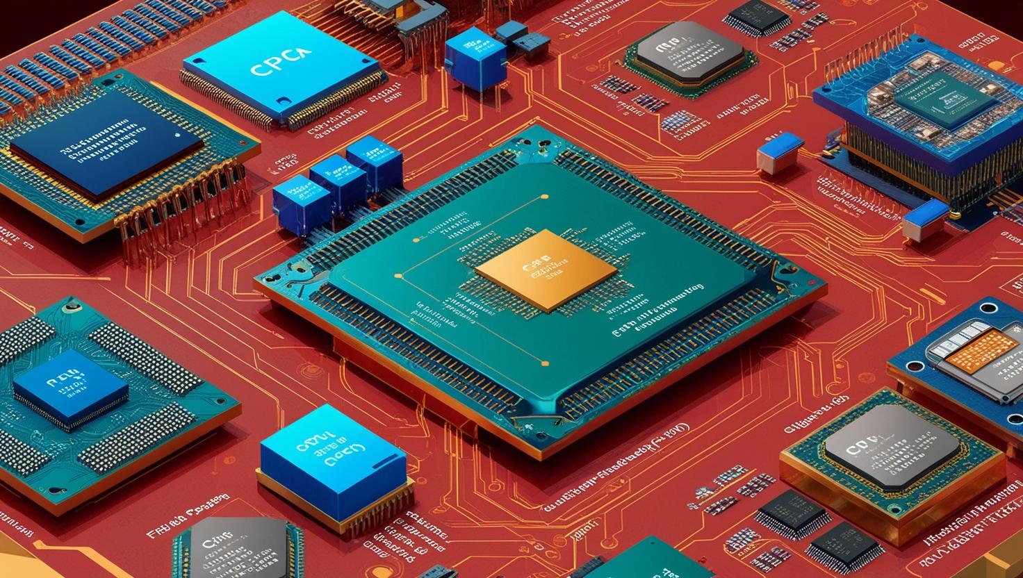
Chiplets are smaller integrated circuits designed to perform specific functions and work together as part of a larger system. Unlike traditional chips, which are manufactured as one large, complex die, chiplets are created as separate modules that can be interconnected within a single package. This modular approach allows manufacturers to mix and match chiplets—each potentially built on different process nodes or technologies—to deliver highly customized and efficient solutions.
The appeal of this design lies in its ability to reduce complexity and improve yields. As transistor density increases, producing large monolithic chips has become expensive and prone to defects. By breaking designs into smaller chiplets, companies can optimize performance while minimizing waste and cost, making the approach more sustainable and economically viable.
Overcoming Moore’s Law
For decades, Moore’s Law—predicting the doubling of transistors on a chip every two years—has driven exponential growth in computing power. However, as physical and material limitations approach their threshold, scaling transistors smaller has become increasingly challenging and costly. The chiplet architecture offers a practical path forward. Instead of relying on continuous miniaturization, innovation now comes from integration—combining multiple chiplets, each dedicated to specific tasks such as processing, graphics, or memory, into a single cohesive system.
This shift from scaling to stacking represents a fundamental change in semiconductor strategy. It allows companies to continue delivering higher performance and efficiency without the need for breakthroughs in lithography or transistor density.
Download PDF Brochure @ https://www.marketsandmarkets.com/pdfdownloadNew.asp?id=131809383
Heterogeneous Integration for High-Performance Computing
One of the most significant advantages of chiplet-based design is heterogeneous integration—the ability to integrate different types of processing units and functions within one package. In high-performance computing (HPC), artificial intelligence (AI), and data center applications, this flexibility is transformative. Designers can combine CPUs, GPUs, AI accelerators, and memory components, each optimized for a specific task, to create systems with unprecedented power and adaptability.
For instance, AI workloads benefit from chiplets dedicated to neural processing, while data center processors can integrate specialized chiplets for network management or security. This modularity supports customized architectures that meet diverse performance and energy efficiency requirements across industries.
Advanced Packaging and Interconnect Technologies
The success of the chiplet revolution relies heavily on advancements in packaging and interconnect technologies. Techniques such as 2.5D interposers, 3D stacking, and fan-out wafer-level packaging have enabled chiplets to communicate at high speeds with minimal latency and power loss. These technologies ensure that the modular approach doesn’t compromise performance compared to traditional monolithic chips.
Furthermore, the emergence of standards like UCIe (Universal Chiplet Interconnect Express) is playing a vital role in ensuring interoperability between chiplets developed by different vendors. By establishing a common framework for data exchange and connectivity, UCIe is paving the way for an open chiplet ecosystem where companies can assemble products using interoperable components from multiple suppliers—similar to how the PC industry evolved in the 1990s.
Economic Efficiency and Time-to-Market Advantages
Beyond performance and flexibility, chiplets offer substantial economic benefits. Producing large chips often leads to low manufacturing yields and high costs, as even minor defects can render entire wafers unusable. By using smaller chiplets, manufacturers improve yields and reduce overall production costs.
Another major advantage is faster time-to-market. Chiplets allow for parallel development, where different teams or even different companies can design separate modules that are later integrated into one system. This collaborative and modular workflow accelerates innovation cycles and allows semiconductor firms to bring products to market more rapidly.
Market Expansion and Applications
The chiplet market is expected to grow from USD 51.94 billion in 2025 to USD 157.23 billion by 2030, at a CAGR of 24.8%. In data centers, chiplets are enabling energy-efficient servers capable of handling complex AI and cloud workloads. Consumer electronics benefit from the ability to integrate high-performance computing in compact devices like smartphones and AR/VR systems. The automotive industry is leveraging chiplets to enhance driver assistance, safety systems, and autonomous vehicle computing platforms.
Even the defense and aerospace sectors are investing in chiplet architectures to improve reliability and adaptability in mission-critical applications. This cross-industry adoption signals that chiplets are not just a technological trend but a foundational shift in how semiconductors will be designed and deployed moving forward.
The Path Toward a Modular Semiconductor Ecosystem
As the chiplet market continues to grow, collaboration across the value chain will be essential. Foundries, design houses, packaging specialists, and software developers must align to create interoperable and efficient systems. Open ecosystems and shared standards will accelerate adoption and innovation, allowing smaller players to compete alongside industry giants.
In the coming years, chiplet integration will play a central role in shaping the next generation of computing—from AI supercomputers to edge devices. The convergence of modular design, advanced packaging, and intelligent software optimization will redefine what’s possible in semiconductor performance and scalability.
Conclusion: The Modular Future of Chip Design
The transition from monolithic to modular chip design marks a pivotal moment in semiconductor history. Chiplets are not just solving the immediate challenges of manufacturing and cost—they are enabling a new level of innovation, collaboration, and design freedom.
As industries demand more powerful and energy-efficient computing solutions, chiplets will remain at the heart of semiconductor evolution. The future of chip design is no longer about cramming more transistors into smaller spaces—it’s about connecting smarter, specialized modules to build limitless possibilities.
Frequently Asked Questions (FAQ): Chiplet Market
1. What is a chiplet?
A chiplet is a small, modular integrated circuit (IC) designed to perform a specific function and operate as part of a larger system. Instead of manufacturing a single, large monolithic chip, designers assemble multiple chiplets inside one package to create a complete system-on-chip (SoC). This modular approach increases design flexibility, improves manufacturing yield, and reduces cost.
2. Why are chiplets important for the semiconductor industry?
Chiplets offer a practical solution to the slowing pace of Moore’s Law. As transistors can no longer be easily shrunk to achieve higher performance, chiplets enable innovation through integration. By combining multiple smaller dies, manufacturers can deliver high-performance systems while reducing complexity and cost.
3. How do chiplets differ from traditional monolithic chips?
Traditional chips are built as one large die, meaning any defect during production can result in significant yield loss. Chiplets divide the chip into smaller, functional blocks that can be manufactured separately and then connected. This reduces waste, enhances performance customization, and allows integration of different process nodes or technologies in one system.