In the ongoing global energy transition, the search for more efficient, flexible, and sustainable alternatives to traditional energy sources has brought thin-film photovoltaic (PV) technology into the spotlight. As governments, corporations, and consumers pursue aggressive decarbonization targets, the thin-film PV market is gaining traction as a viable disruptor to the long-dominant crystalline silicon (c-Si) solar technology. With rapid advances in materials science, production processes, and real-world performance, thin-film PV is no longer a secondary player—it’s emerging as a core component of solar’s future.
Understanding Thin-Film Photovoltaic Technology
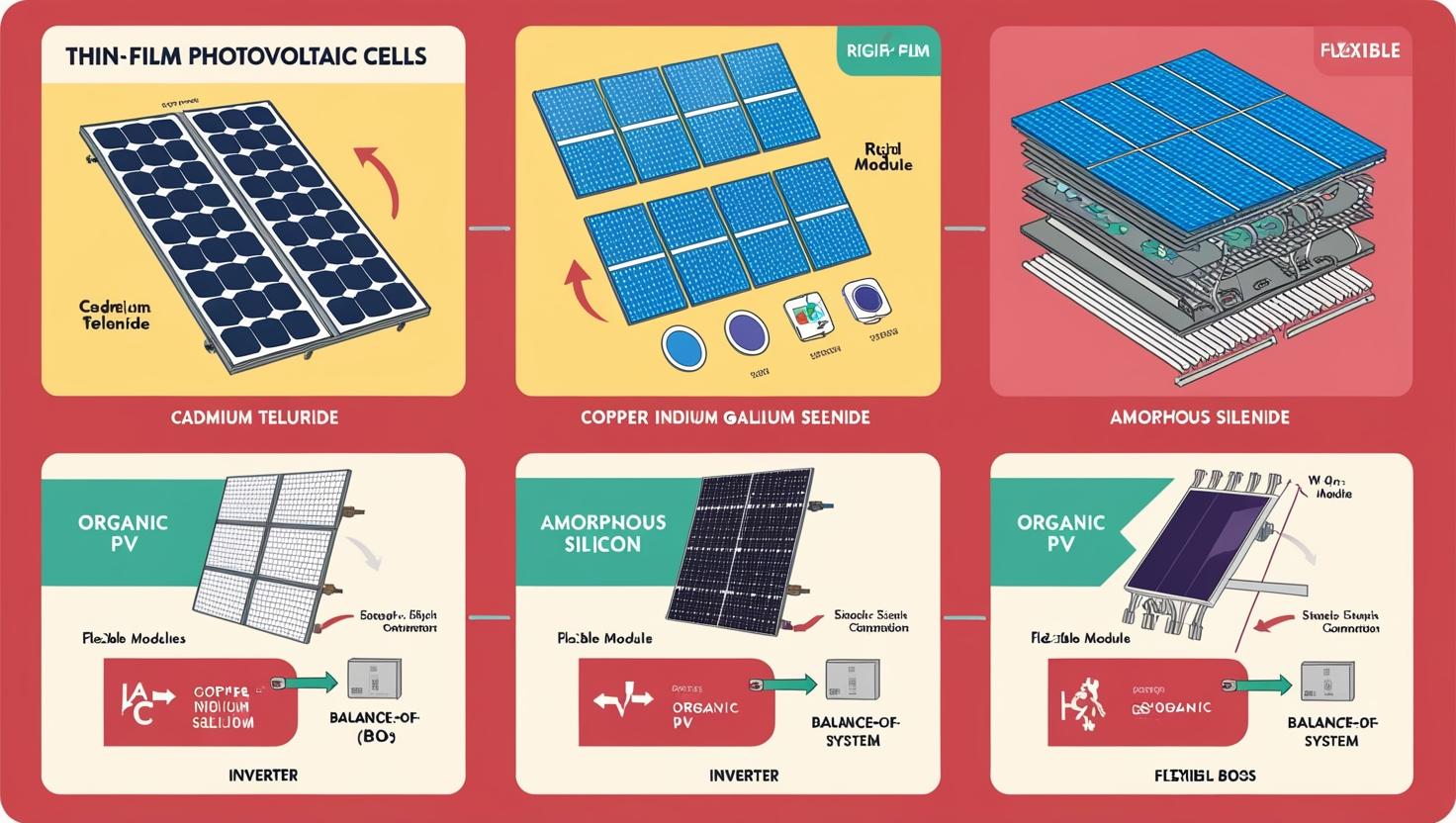
Thin-film photovoltaics are made by depositing one or more layers of light-absorbing materials onto a substrate such as glass, plastic, or metal. Unlike traditional silicon panels, which are bulky and rigid, thin-film cells are extremely lightweight and flexible. This difference in structure enables the technology to be applied in areas and formats where conventional panels are impractical or too heavy. Among the most commonly used materials in thin-film PV are Cadmium Telluride (CdTe), Copper Indium Gallium Selenide (CIGS), and Amorphous Silicon (a-Si), each offering a unique balance of efficiency, cost, and environmental compatibility.
Flexibility and Lightweight Design: A Competitive Advantage
One of the most transformative advantages of thin-film PV is its physical flexibility. These modules can bend, wrap, and adapt to a wide range of surfaces—something crystalline silicon cannot achieve. As a result, thin-film PV opens doors for entirely new applications such as solar-integrated facades, curved rooftops, agricultural structures, tents, and even vehicles. The reduced weight of thin-film modules also significantly lowers installation costs and structural support requirements, especially in retrofitting projects and lightweight architecture.
Download PDF Brochure @ https://www.marketsandmarkets.com/pdfdownloadNew.asp?id=31
Performance Beyond Efficiency Ratings
Although crystalline silicon still dominates in lab-tested efficiency metrics, thin-film technologies have demonstrated superior performance under real-world conditions. Thin-film panels operate more efficiently in low-light environments, perform better at high temperatures, and are less affected by shading or partial obstruction. This makes them particularly well-suited for urban areas, high-temperature regions, and places where sunlight is intermittent. Cadmium Telluride modules, in particular, have achieved notable commercial success due to their durability, cost-effectiveness, and adaptability in utility-scale solar installations.
Market Momentum and Emerging Applications
The thin-film PV market is experiencing significant growth as new use cases continue to emerge. One of the most promising areas is building-integrated photovoltaics (BIPV), where thin-film solar elements are embedded directly into construction materials such as windows, roofing tiles, and facades. This approach allows buildings to generate their own clean energy without relying on separate rooftop panels. Additionally, sectors like aerospace, military, transportation, and consumer electronics are increasingly investing in portable or flexible thin-film solar solutions for off-grid energy generation.
Driving Forces Behind the Market Surge
Several macro and micro-level trends are converging to push thin-film PV forward. On a policy level, national governments and international climate frameworks are providing subsidies, incentives, and mandates that support solar diversification beyond silicon. At the same time, rising demand for lightweight, mobile, and aesthetically integrated solar systems has encouraged manufacturers to innovate rapidly. The growing importance of energy access in remote and underserved areas has also positioned thin-film PV as a critical solution due to its portability and ease of deployment.
Innovation in Manufacturing and Sustainability
Manufacturing techniques for thin-film PV are becoming more efficient and scalable, particularly through roll-to-roll processing and automated deposition methods. These processes reduce material waste and lower the overall carbon footprint of production. Additionally, advances in non-toxic and abundant materials are addressing environmental concerns associated with some thin-film technologies, such as cadmium content. The focus on circular design and recyclability is also gaining attention, as manufacturers aim to meet both environmental and regulatory standards.
Challenges to Widespread Adoption
Despite its promise, thin-film PV still faces certain hurdles. The initial investment required for new manufacturing facilities and research remains high. Thin-film also faces competitive pressure from increasingly efficient and low-cost silicon modules, especially in utility-scale projects where price-per-watt is the dominant metric. Furthermore, some thin-film materials rely on rare or regulated elements, which can create supply chain constraints. However, as innovation continues and niche markets scale, these challenges are being actively addressed by key players in the industry.
A Complementary Role in the Solar Ecosystem
Rather than viewing thin-film PV as a replacement for silicon-based solar, many experts see it as a complementary solution. While crystalline silicon will likely continue to dominate large-scale solar farms, thin-film’s unique properties make it ideal for applications where flexibility, light weight, or surface integration are essential. The coexistence of both technologies enables a more versatile and resilient solar energy ecosystem—one capable of meeting diverse energy demands around the world.
Outlook: A Disruptive Force with Expanding Influence
Looking ahead to 2029 and beyond, thin-film photovoltaic technology is well-positioned to disrupt traditional solar markets—not through direct competition alone, but by expanding the boundaries of where and how solar energy can be applied. With increasing investments, rising demand for mobile and integrated energy solutions, and growing emphasis on sustainable manufacturing, thin-film PV is not just an alternative—it’s a strategic enabler in the transition to a more decentralized and decarbonized energy future.
Frequently Asked Questions (FAQ) – Thin-Film Photovoltaic (PV) Market
Q1: What is thin-film photovoltaic technology?
Thin-film photovoltaic technology involves depositing very thin layers of photovoltaic material onto substrates like glass, plastic, or metal. This differs from traditional silicon solar panels, offering lightweight and flexible solar solutions.
Q2: How does thin-film PV differ from traditional crystalline silicon solar panels?
Thin-film PV panels are lighter, flexible, and can be applied to curved or irregular surfaces. While crystalline silicon panels typically have higher efficiency, thin-film performs better in low-light and high-temperature conditions.
Q3: What are the main types of thin-film PV materials?
The most common types are Cadmium Telluride (CdTe), Copper Indium Gallium Selenide (CIGS), and Amorphous Silicon (a-Si), each with unique properties suited for different applications.
Q4: What are the advantages of thin-film PV?
Advantages include flexibility, lightweight design, better performance in shade or heat, lower production energy requirements, and the ability to integrate with building materials and portable devices.