The Hybrid Bonding Market Size is witnessing significant expansion as the semiconductor industry accelerates toward advanced packaging technologies. With increasing demand for higher performance, miniaturization, and energy efficiency, hybrid bonding has emerged as a critical innovation enabling next-generation chip integration.
The global hybrid bonding market is projected to reach USD 633.9 million by 2032 from USD 164.7 million in 2025, registering a CAGR of 21.2% from 2025 to 2032
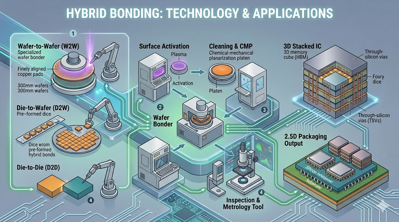
At its core, hybrid bonding allows direct copper-to-copper and dielectric-to-dielectric connections without the need for traditional solder bumps. This results in improved electrical performance, higher interconnect density, and enhanced thermal efficiency. As a result, the Hybrid Bonding Market Size is expected to grow rapidly, driven by its ability to support complex architectures such as 3D ICs and chiplet-based designs.
One of the key factors fueling the Hybrid Bonding Market Size is the rising demand for high-performance computing (HPC), artificial intelligence (AI), and data centers. These applications require advanced semiconductor solutions capable of handling massive data processing with minimal latency. Hybrid bonding enables tighter integration of components, which significantly boosts speed and bandwidth while reducing power consumption.
Another major driver of the Hybrid Bonding Market Size is the evolution of heterogeneous integration. By combining different types of chips—such as logic, memory, and sensors—into a single package, manufacturers can achieve greater functionality and flexibility. Hybrid bonding plays a crucial role in enabling this level of integration, making it a cornerstone of modern semiconductor packaging strategies.
Download PDF Brochure @ https://www.marketsandmarkets.com/pdfdownloadNew.asp?id=2641237
The growth of consumer electronics, including smartphones, wearables, and gaming devices, is also contributing to the expansion of the Hybrid Bonding Market Size. As devices become more compact and powerful, the need for advanced interconnect technologies continues to rise. Hybrid bonding helps meet these demands by enabling smaller form factors without compromising performance.
In addition, the adoption of 5G technology and the proliferation of IoT devices are further accelerating the Hybrid Bonding Market Size. These technologies require efficient, high-speed chips capable of handling large volumes of data. Hybrid bonding supports these requirements by improving signal integrity and reducing parasitic losses.
Despite its promising growth, the Hybrid Bonding Market Size faces certain challenges, including high manufacturing complexity and significant initial investment costs. The technology requires ultra-precise alignment and clean manufacturing environments, which can increase production costs. However, ongoing research and development efforts are expected to reduce these barriers over time.
Looking ahead, the Hybrid Bonding Market Size is poised for substantial growth as semiconductor companies continue to push the boundaries of innovation. With increasing adoption in advanced packaging, the technology is expected to become a standard in future chip manufacturing processes.
FAQs
1. What is driving the growth of the Hybrid Bonding Market Size?
The Hybrid Bonding Market Size is growing due to increasing demand for advanced semiconductor packaging, high-performance computing, AI applications, and the need for miniaturized, high-efficiency chips.
2. How does hybrid bonding differ from traditional bonding methods?
Unlike traditional solder-based bonding, hybrid bonding enables direct copper-to-copper connections, resulting in better electrical performance, higher density, and improved thermal management.
3. Which industries are contributing to the Hybrid Bonding Market Size?
Industries such as data centers, consumer electronics, automotive, telecommunications, and IoT are major contributors to the Hybrid Bonding Market Size.
4. What are the challenges in the Hybrid Bonding Market Size growth?
Key challenges include high production costs, complex manufacturing processes, and the need for ultra-precise alignment and advanced fabrication facilities.
5. What is the future outlook of the Hybrid Bonding Market Size?
The Hybrid Bonding Market Size is expected to grow significantly in the coming years, driven by advancements in semiconductor technologies and increasing adoption of 3D integration and chiplet architectures.