The semiconductor industry is entering a new era where traditional scaling alone is no longer sufficient to meet performance, power, and density requirements. As devices demand higher bandwidth, lower latency, and greater energy efficiency, advanced packaging has become a central driver of innovation. At the core of this transformation lies hybrid bonding market a technology that is rapidly reshaping how chips are interconnected and integrated. The hybrid bonding market is emerging as a critical enabler of next-generation semiconductor architectures, powering everything from high-performance computing to AI and advanced memory solutions.
Understanding Hybrid Bonding
Hybrid bonding is an advanced interconnect technology that combines direct copper-to-copper bonding with dielectric-to-dielectric bonding at extremely fine pitches. Unlike traditional solder-based approaches, hybrid bonding enables ultra-dense interconnects with minimal signal loss, improved electrical performance, and reduced power consumption. This capability makes it especially well-suited for advanced logic, memory stacking, and heterogeneous integration.
By eliminating micro-bumps and reducing interconnect distances, hybrid bonding allows chip designers to move beyond the limitations of conventional packaging techniques.
he global hybrid bonding market is projected to reach USD 633.9 million by 2032 from USD 164.7 million in 2025, registering a CAGR of 21.2% from 2025 to 2032.
Key Bonding Approaches Driving Adoption
The market encompasses several bonding configurations, each serving distinct manufacturing and design needs:
-
Wafer-to-Wafer (W2W) Bonding: Ideal for high-volume, uniform devices such as memory stacks, offering excellent alignment accuracy and cost efficiency at scale.
-
Die-to-Wafer (D2W) Bonding: Enables greater flexibility by bonding known-good dies onto wafers, improving yields for complex logic and heterogeneous integration.
-
Die-to-Die (D2D) Bonding: Supports advanced modular designs where individual dies are bonded together, unlocking new chiplet-based architectures.
These approaches allow manufacturers to balance yield, flexibility, and cost depending on application requirements.
Equipment Ecosystem Supporting Hybrid Bonding
The successful adoption of hybrid bonding relies on a sophisticated toolchain designed to achieve atomic-level precision. Key equipment segments include:
-
Wafer Bonders: Delivering ultra-precise alignment and bonding accuracy
-
Surface Preparation Tools: Ensuring contamination-free, bond-ready surfaces
-
Inspection & Metrology Tools: Verifying alignment, bond integrity, and defect detection
-
Cleaning & CMP Systems: Enabling planarization and surface uniformity critical for bonding success
Advancements across this equipment ecosystem are helping manufacturers achieve higher yields and throughput, accelerating the transition from pilot lines to high-volume production.
Download PDF Brochure @ https://www.marketsandmarkets.com/pdfdownloadNew.asp?id=2641237
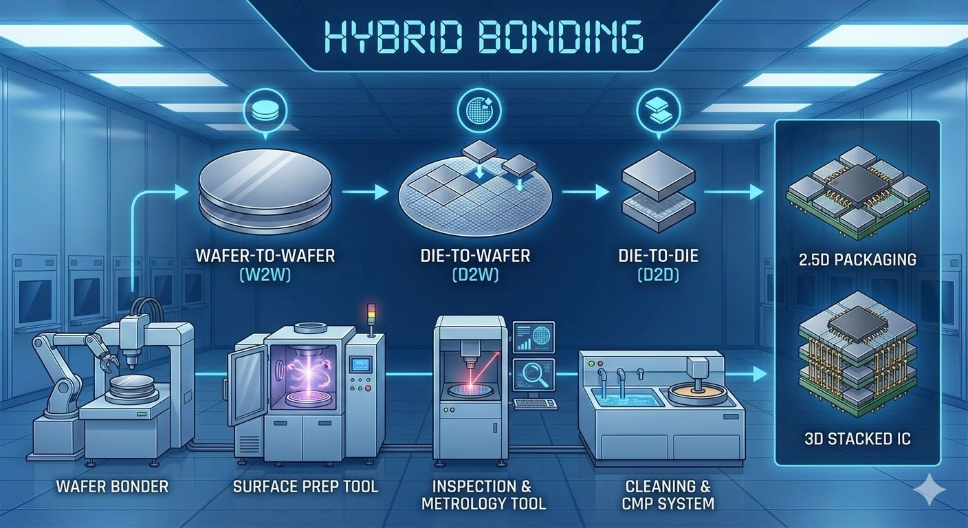
Enabling 2.5D Packaging and 3D Stacked ICs
Hybrid bonding plays a pivotal role in enabling 2.5D packaging and 3D stacked integrated circuits (ICs). In 2.5D architectures, it supports high-density interconnects between dies and interposers, improving bandwidth and performance. In 3D stacked ICs, hybrid bonding enables vertical integration of logic and memory with unprecedented interconnect density.
These capabilities are essential for applications such as AI accelerators, high-bandwidth memory (HBM), advanced processors, and data-center-class computing, where performance and energy efficiency are paramount.
Market Drivers and Industry Momentum
Several forces are accelerating growth in the hybrid bonding market:
-
Rising demand for AI, machine learning, and high-performance computing
-
Increasing adoption of chiplet-based designs
-
Limitations of traditional scaling at advanced nodes
-
Need for higher interconnect density and lower power consumption
Leading semiconductor manufacturers and foundries are investing heavily in hybrid bonding to gain a competitive edge, signaling strong long-term market momentum.
Looking Ahead
As semiconductor architectures become more complex and performance demands continue to rise, hybrid bonding is transitioning from an emerging technology to a manufacturing necessity. Its ability to deliver fine-pitch interconnects, improved electrical performance, and scalable integration positions it at the heart of future advanced packaging strategies.
The hybrid bonding market is not just supporting the next generation of chips—it is redefining how they are built. In an industry driven by precision and innovation, hybrid bonding stands out as a foundational technology powering the future of semiconductor integration.
Hybrid Bonding Market – FAQ
1. What is hybrid bonding in semiconductor manufacturing?
Hybrid bonding is an advanced interconnect technology that combines direct copper-to-copper bonding with dielectric-to-dielectric bonding. It enables ultra-fine interconnect pitches without traditional solder bumps, resulting in higher bandwidth, lower power consumption, and improved performance.
2. Why is hybrid bonding important for advanced packaging?
As traditional transistor scaling slows, advanced packaging has become critical for performance gains. Hybrid bonding allows higher interconnect density and shorter signal paths, making it essential for 2.5D packaging, 3D stacked ICs, and chiplet-based architectures.
3. What are the main types of hybrid bonding?
- Wafer-to-Wafer (W2W): High-volume, cost-efficient bonding for uniform dies
- Die-to-Wafer (D2W): Flexible integration of known-good dies for better yield
- Die-to-Die (D2D): Modular bonding for advanced heterogeneous designs
- Each type serves different manufacturing and design requirements.
4. What equipment is required for hybrid bonding?
The hybrid bonding process relies on a specialized toolchain, including:
- Wafer bonders
- Surface preparation tools
- Inspection and metrology systems
- Cleaning and CMP (Chemical Mechanical Planarization) systems
- Precision and cleanliness at every step are critical to achieving high yields.