The EUV mask market is experiencing a notable surge in growth as the global semiconductor industry intensifies its push toward advanced process nodes. With technology nodes shrinking below 7nm and chipmakers racing to produce faster, more efficient microprocessors, EUV lithography has become a critical enabler. At the heart of this transition lies the EUV mask market, which plays a pivotal role in ensuring the success and precision of next-generation chip manufacturing.
The Role of EUV Masks in Advanced Lithography
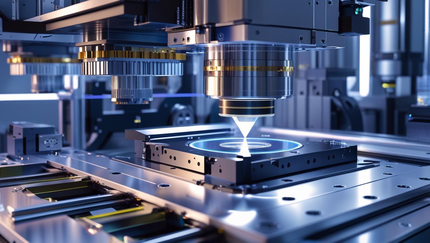
EUV (Extreme Ultraviolet) lithography is a highly advanced technology that uses short-wavelength light (13.5 nm) to etch intricate patterns onto silicon wafers. This allows for much finer resolutions compared to traditional deep ultraviolet (DUV) techniques. However, to make EUV lithography work effectively, ultra-precise and defect-free masks are essential. The EUV mask market provides these complex optical components, which serve as the blueprint for high-performance chip fabrication.
EUV masks differ significantly from conventional photomasks. They are multilayered, reflective, and highly sensitive to contamination or pattern distortion. As the industry moves toward sub-5nm and 3nm nodes, the demand for ultra-accurate, durable, and defect-free masks is increasing rapidly—propelling the growth of the EUV mask market.
Regional Insights and Competitive Landscape
Asia-Pacific currently leads the EUV mask market, driven by strong demand from major chipmakers in Taiwan, South Korea, and China. TSMC and Samsung are at the forefront of EUV adoption, using it in commercial production of 5nm and 3nm chips. North America, with companies like Intel and GlobalFoundries, is also investing heavily in EUV-based manufacturing, contributing to a robust outlook for the EUV mask market.
Leading players in the EUV mask market include ASML, Toppan Photomasks, Hoya Corporation, DNP, and Photronics, among others. These companies are innovating in areas such as mask blank production, pellicle design, and defect inspection—ensuring that they stay competitive as demand scales.
Future Outlook
The EUV mask market is poised for continued expansion as the semiconductor sector moves further into the realm of advanced nodes. The EUV lithography market is expected to reach USD 22.69 billion by 2029 from USD 12.18 billion in 2024, at a CAGR of 13.2% during the 2024-2029 period. increasing applications in mobile computing, automotive electronics, and data centers.
As Moore’s Law continues to evolve, the complexity and importance of EUV masks will only grow. Stakeholders in the EUV mask market who focus on innovation, defect control, and manufacturing efficiency will be well-positioned to capture emerging opportunities.
Download PDF Brochure @ https://www.marketsandmarkets.com/pdfdownloadNew.asp?id=241564826
Key Market Drivers
The primary driver of the EUV mask market is the global semiconductor industry’s transition to advanced process nodes, particularly at 7nm, 5nm, and below. As integrated circuits become more densely packed and power-efficient, the need for extreme ultraviolet (EUV) lithography grows. EUV lithography enables finer patterning on silicon wafers, and EUV masks are essential components in this process.
Another major driver is the rising demand for high-performance computing (HPC), AI accelerators, and 5G infrastructure, which require chips manufactured with advanced lithography techniques. As the end-user market expands, particularly in smartphones, data centers, and electric vehicles, chipmakers must produce more chips using EUV technology—boosting demand in the EUV mask market.
The increased investment in semiconductor fabs by major players like TSMC, Samsung, Intel, and new entrants in the U.S., Europe, and Asia-Pacific also fuels EUV mask consumption. As more foundries adopt EUV tools for volume production, the demand for photomask blanks, pellicles, and inspection tools increases proportionally.
Finally, the push for greater efficiency and reduced design complexity in advanced chip manufacturing continues to drive innovation in EUV mask design and materials, supporting long-term market growth.
Benefits of EUV Masks in Semiconductor Manufacturing
EUV masks offer significant advantages that are critical to the ongoing advancement of semiconductor technology. First and foremost, they enable extreme precision in patterning, allowing chipmakers to etch incredibly fine features onto silicon wafers. This precision is essential for fabricating smaller, faster, and more energy-efficient chips that meet the demands of modern electronics.
Another key benefit is the ability to support advanced process nodes, such as 7nm, 5nm, and beyond, which traditional lithography methods cannot achieve effectively. EUV masks facilitate these cutting-edge nodes, helping to sustain Moore’s Law and drive innovation across industries.
EUV masks also contribute to higher manufacturing throughput by enabling single-exposure patterning of complex chip designs, reducing the number of processing steps compared to older multi-patterning techniques. This leads to lower production costs and shorter time-to-market for semiconductor products.
Additionally, the use of EUV masks enhances device performance and power efficiency, as smaller feature sizes translate to faster switching speeds and reduced energy consumption in chips. This benefit is especially important for sectors like mobile computing, AI, automotive electronics, and data centers.
Lastly, EUV masks support scalability and future-proofing of semiconductor fabrication. As chip architectures become more complex and demand grows for specialized functions, EUV masks offer the flexibility and accuracy needed to meet evolving technological requirements.
The key players in EUV lithography are ASML (Netherlands), Carl Zeiss AG (Germany), NTT Advanced Technology Corporation (Japan), KLA Corporation (US), ADVANTEST CORPORATION (Japan), Ushio Inc. (Japan), SUSS MicroTec SE (Germany), AGC Inc. (Japan), Lasertec Corporation (Japan), TOPPAN Inc. (Japan), Energetiq Technology, Inc. (Japan), NuFlare Technology Inc. (US), Photronics, Inc. (Japan), HOYA Corporation (Japan), TRUMPF (Germany), Rigaku Holdings Corporation (Japan), Edmund Optics Inc. (US), Imagine Optic (France), Applied Materials, Inc. (US), Park Systems (South Koria), EUV Tech (US), Mloptic Crop. (China), MKS Instruments (US), Brooks Automation (US), and Pfeiffer Vacuum GmbH (Germany).
Frequently Asked Questions (FAQ)
1. What is an EUV mask?
An EUV (Extreme Ultraviolet) mask is a specialized photomask used in EUV lithography to transfer intricate circuit patterns onto silicon wafers during semiconductor manufacturing. It is reflective and multilayered, designed to work with the short wavelength of EUV light.
2. Why is the EUV mask market growing?
The EUV mask market is growing due to the semiconductor industry’s shift towards smaller, more advanced process nodes (7nm and below), which require EUV lithography. Increasing demand for high-performance chips in AI, 5G, and HPC is also fueling this growth.
3. How does an EUV mask differ from traditional photomasks?
Unlike traditional photomasks used in deep ultraviolet (DUV) lithography, EUV masks are reflective rather than transmissive and consist of multiple layers. They are more complex to manufacture and require stricter defect control due to the shorter wavelength of EUV light.