The global semiconductor industry is undergoing a major architectural shift driven by the rise of chiplet-based design. As monolithic chips reach physical and economic limits, chiplets offer a powerful alternative by breaking complex systems into smaller, modular dies that work together inside a single package. This modularization delivers superior yield, faster performance scaling, and reduced manufacturing costs, while enabling unprecedented design flexibility. As the demand for AI, cloud computing, and advanced edge applications surges, chiplets are becoming a foundational technology for next-generation processors.
The Growing Importance of Chiplet-Based Processors
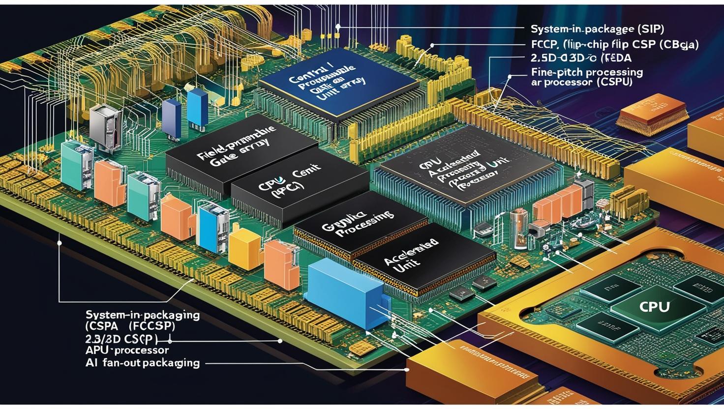
Chiplet architectures are reshaping how modern processors are developed by enabling the integration of multiple specialized dies within a unified system. Instead of relying on a single large silicon die—which can be expensive, difficult to produce, and prone to defects—manufacturers can now combine compact, optimized chiplets that handle distinct functions. This approach allows CPUs to scale core counts more efficiently, GPUs to achieve superior parallelism and bandwidth, and SoCs to incorporate a diverse mix of compute, graphics, and AI engines in a streamlined manner. The emergence of AI-specific ASIC co-processors further highlights the role of chiplets in accelerating machine learning tasks that demand extremely high throughput. In fields ranging from high-performance computing to data center workloads and mobile devices, chiplet processors are enabling faster innovation cycles and enhanced performance density.
Download PDF Brochure @ https://www.marketsandmarkets.com/pdfdownloadNew.asp?id=131809383
The Role of Advanced Packaging Technologies
Advanced packaging has become the critical enabler that allows chiplets to function as a unified, high-performance system. Technologies such as System-in-Package, Fan-Out packaging, wafer-level chip scale packaging, and flip-chip approaches each contribute unique advantages in power efficiency, thermal management, and signal integrity. Even more transformative are 2.5D and 3D packaging techniques, which allow multiple chiplets to be placed on a silicon interposer or vertically stacked, dramatically reducing communication latency and increasing bandwidth. This is especially crucial for AI accelerators and GPUs, which rely on tight coupling with high-bandwidth memory. Packaging innovation ensures that despite being physically separate pieces of silicon, chiplets can communicate seamlessly and behave like a single, cohesive processor.
Market Forces Driving Chiplet Adoption
Several industry dynamics are accelerating the adoption of chiplet-based architectures. The exponential growth of AI workloads, especially in data centers and edge computing, places enormous demands on compute density and energy efficiency that traditional chip designs struggle to meet. Chiplets also offer economic advantages by allowing companies to fabricate smaller dies, improving yield rates and lowering production costs. Their modular nature allows designers to mix technologies from different process nodes, enabling optimal combinations of digital logic, analog components, and memory within the same package. This heterogeneity significantly reduces time-to-market and encourages rapid innovation, allowing manufacturers to scale performance more dynamically in response to evolving market needs.
Ecosystem Expansion and Industry Leadership
Major semiconductor companies are driving the evolution of chiplet technology through substantial investments in advanced packaging and multi-die integration. AMD has led the industry in commercializing chiplet-based CPUs and GPUs, demonstrating the architecture’s scalability and performance benefits. Intel has accelerated its strategy with EMIB and Foveros, which support both 2.5D and 3D integration with high-density interconnects. Foundries like TSMC play an equally pivotal role by offering packaging platforms such as CoWoS and InFO, which provide the manufacturing backbone for chiplet-dependent designs. At the same time, AI-centric semiconductor firms are leveraging chiplets to deliver specialized training and inference accelerators, pushing performance boundaries across industries including cloud AI, autonomous vehicles, and scientific research.
Toward Standardized and Interoperable Chiplet Architectures
One of the most transformative developments in the chiplet market is the movement toward open standards that allow dies from different vendors to interoperate seamlessly. The Universal Chiplet Interconnect Express (UCIe) standard represents a significant step forward in creating a multi-vendor chiplet ecosystem. With standardized physical and logical interfaces, manufacturers may soon be able to integrate chiplets like modular building blocks, combining best-in-class components from multiple suppliers. This trend is expected to enhance collaboration across the semiconductor value chain, reduce development barriers for emerging companies, and accelerate innovation at a system level.
Future Outlook: Chiplets as the Foundation of Semiconductor Innovation
The future of semiconductor technology is increasingly tied to the evolution of chiplet-based architectures. As traditional Moore’s Law scaling slows, chiplets offer a viable pathway to continue advancing compute performance, energy efficiency, and system specialization. Their ability to support heterogeneous integration will be vital for emerging domains such as quantum computing, advanced AI, autonomous machines, and next-generation telecommunications. With rapid advancements in packaging, interconnect technology, and ecosystem standardization, chiplets are set to become the default design paradigm for future processors across consumer electronics, enterprise hardware, and cloud infrastructure.
FAQ: Chiplet Market
1. Why is the chiplet market considered a major investment opportunity?
The chiplet market is becoming one of the fastest-growing segments in semiconductors due to its ability to overcome the scaling limits of monolithic chips. As AI, cloud computing, data centers, and edge devices demand higher performance and lower power consumption, chiplets provide the most cost-effective and scalable architectural solution. This structural shift positions chiplet technology as a long-term growth engine for the global semiconductor industry.
2. What industries are driving demand for chiplet-based solutions?
The strongest demand comes from AI data centers, high-performance computing, gaming, networking equipment, 5G infrastructure, defense electronics, and advanced consumer devices. AI workloads in particular require massive parallelism and memory bandwidth—conditions under which chiplets excel. The electrification of vehicles and the rise of autonomous driving are also creating new growth pathways.
3. How do chiplets provide a competitive advantage over traditional monolithic chips?
Chiplets significantly improve manufacturing yield, reduce production costs, and allow companies to mix different process nodes within a single package. They enable higher compute density, shorter design cycles, and better thermal performance compared to monolithic chips. This makes them particularly attractive for companies seeking rapid innovation without escalating manufacturing complexity or cost.