
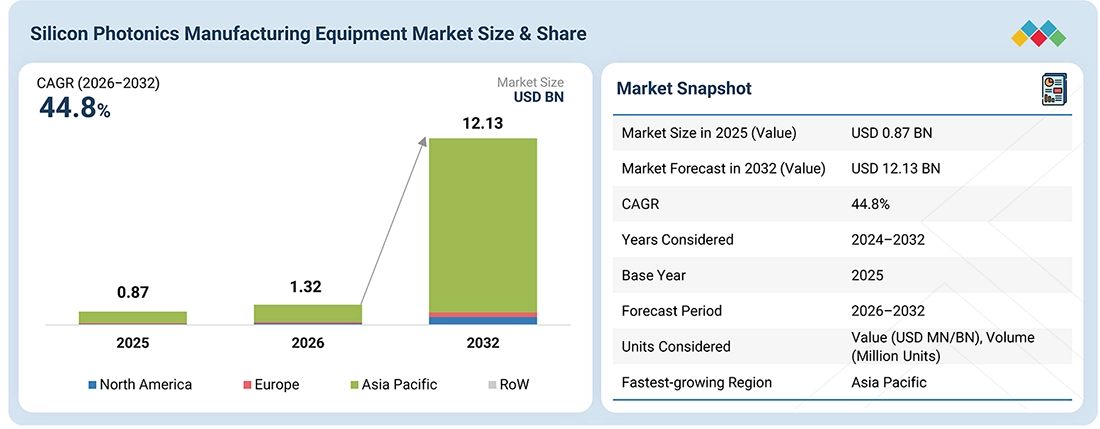
Growing Packaging Investments Accelerate Silicon Photonics Adoption
Increasing investments in advanced semiconductor packaging are supporting the growth of silicon photonics manufacturing as demand for high-speed, energy-efficient communication technologies continues to expand. The rapid development of artificial intelligence (AI), cloud computing, high-performance computing, and telecommunications infrastructure is creating demand for optical components capable of transferring large volumes of data with low latency. Silicon photonics is gaining importance because it integrates optical functions with semiconductor technologies, enabling compact and high-performance communication solutions. Consequently, semiconductor manufacturers and packaging specialists are investing in advanced manufacturing equipment and integration technologies to support commercial production.
Advanced packaging plays a critical role in silicon photonics because optical components must be precisely connected with electronic circuits, optical fibers, lasers, and other semiconductor devices. Unlike conventional electronic packaging, photonic packaging requires accurate optical alignment to maintain efficient light transmission and minimize signal losses. These requirements are encouraging investments in precision bonding, automated assembly, optical inspection, and advanced testing systems. As silicon photonics applications expand, packaging innovation is becoming an important factor influencing manufacturing capacity and product reliability.
Download PDF Brochure @ https://www.marketsandmarkets.com/pdfdownloadNew.asp?id=189563536
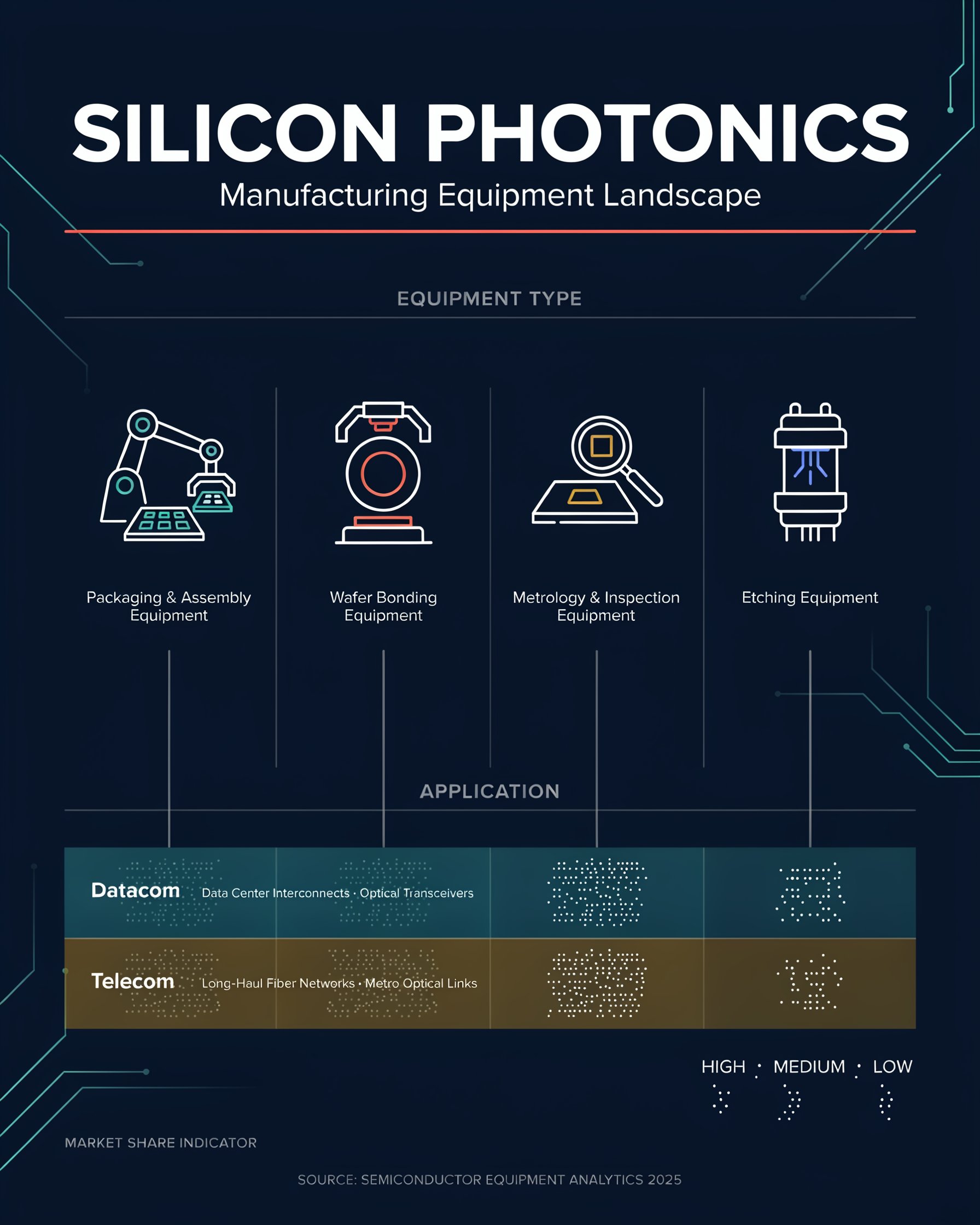
AI Data Center Expansion Strengthens Packaging Demand
The rapid expansion of AI data centers is creating substantial opportunities for silicon photonics manufacturing. AI training and inference workloads require continuous communication between processors, accelerators, memory systems, and networking equipment. Increasing computing densities are placing pressure on conventional electrical interconnects, particularly in applications requiring high bandwidth and efficient power management.
Silicon photonics provides an alternative through optical interconnects that support high-speed data transmission. Photonic integrated circuits and optical transceivers are increasingly being explored for data center networking and high-performance computing applications. However, achieving the required performance depends on effective integration of optical and electronic components.
Advanced packaging investments are helping manufacturers address these requirements. Precision die placement, wafer-level packaging, optical fiber attachment, and automated alignment technologies support the development of compact photonic devices. Packaging equipment suppliers are also focusing on improved manufacturing accuracy and repeatability to support growing production volumes. As AI infrastructure investments increase, demand for advanced packaging solutions is expected to strengthen.
Co-Packaged Optics Creates New Manufacturing Opportunities
Co-packaged optics is emerging as an important development in advanced semiconductor packaging. This approach places optical components closer to electronic switching or processing chips, helping reduce the distance that high-speed electrical signals must travel. It has the potential to improve bandwidth density and energy efficiency in demanding networking and computing environments.
The manufacturing of co-packaged optical systems requires sophisticated packaging processes. Optical components, electronic chips, and fiber connections must be integrated within compact assemblies while maintaining thermal stability and reliable signal transmission. These requirements are encouraging investments in advanced bonding, precision placement, substrate processing, and optical testing equipment.
Semiconductor manufacturers and packaging providers are exploring new integration approaches to improve production scalability. Equipment suppliers are developing automated assembly systems that can support accurate component placement and consistent packaging quality. As commercial adoption of co-packaged optics develops, these technologies could create additional opportunities for specialized silicon photonics manufacturing equipment providers.
Inquiry Before Buying @ https://www.marketsandmarkets.com/Enquiry_Before_BuyingNew.asp?id=189563536
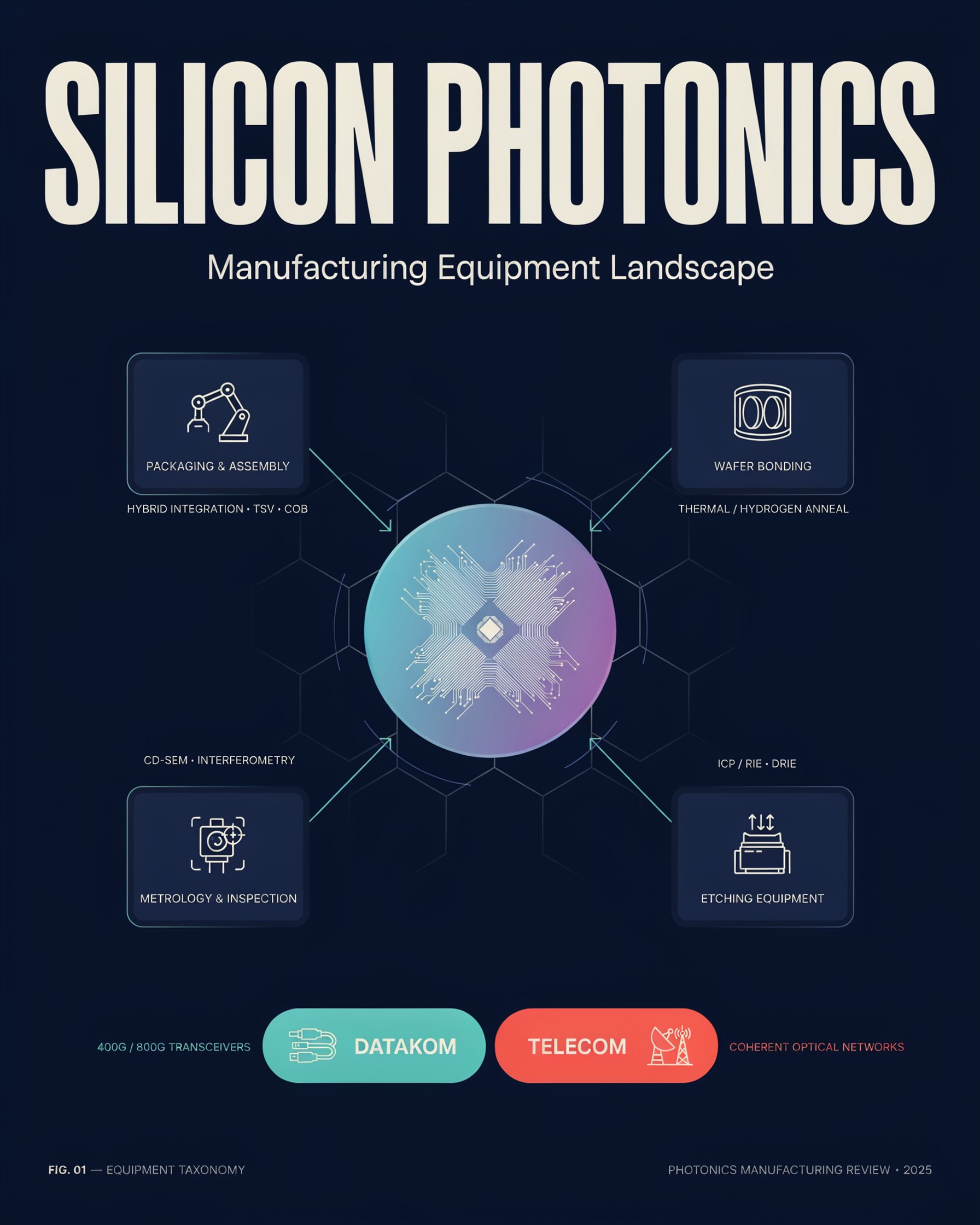
Heterogeneous Integration Strengthens Packaging Innovation
Heterogeneous integration is another important factor supporting investments in advanced semiconductor packaging. Silicon photonics devices may require the integration of silicon-based optical circuits with other semiconductor materials, including indium phosphide, to support different optical functions. Combining multiple materials and components can enable improved device performance and compact system architectures.
However, heterogeneous integration introduces manufacturing challenges involving material compatibility, bonding accuracy, thermal management, and electrical connectivity. Advanced packaging technologies help address these requirements by enabling different components to be integrated within a single device or package.
Manufacturers are investing in hybrid bonding, wafer bonding, precision die attachment, and advanced inspection systems to improve integration quality. These processes require specialized equipment capable of maintaining consistent alignment and minimizing defects. Continued development of heterogeneous integration is expected to strengthen demand for advanced packaging technologies across silicon photonics production.
Automated Assembly and Optical Testing Improve Production Efficiency
The increasing complexity of photonic devices is encouraging manufacturers to adopt automated packaging and testing systems. Optical components require accurate alignment between waveguides, fibers, and other optical interfaces. Manual assembly processes can introduce variations that affect optical coupling efficiency and production consistency.
Automated optical alignment systems help improve positioning accuracy and reduce assembly errors. Precision bonding and die placement equipment support reliable integration of optical and electronic components. Advanced inspection technologies also enable manufacturers to identify defects during packaging and improve overall product quality.
Testing is equally important because photonic devices must meet requirements related to insertion loss, optical power, wavelength performance, and thermal reliability. Automated testing platforms allow manufacturers to evaluate device characteristics more efficiently. Integrating testing into packaging workflows can help reduce production delays and improve manufacturing yields.
View detailed Table of Content here – https://www.marketsandmarkets.com/Market-Reports/silicon-photonics-manufacturing-equipment-market-189563536.html
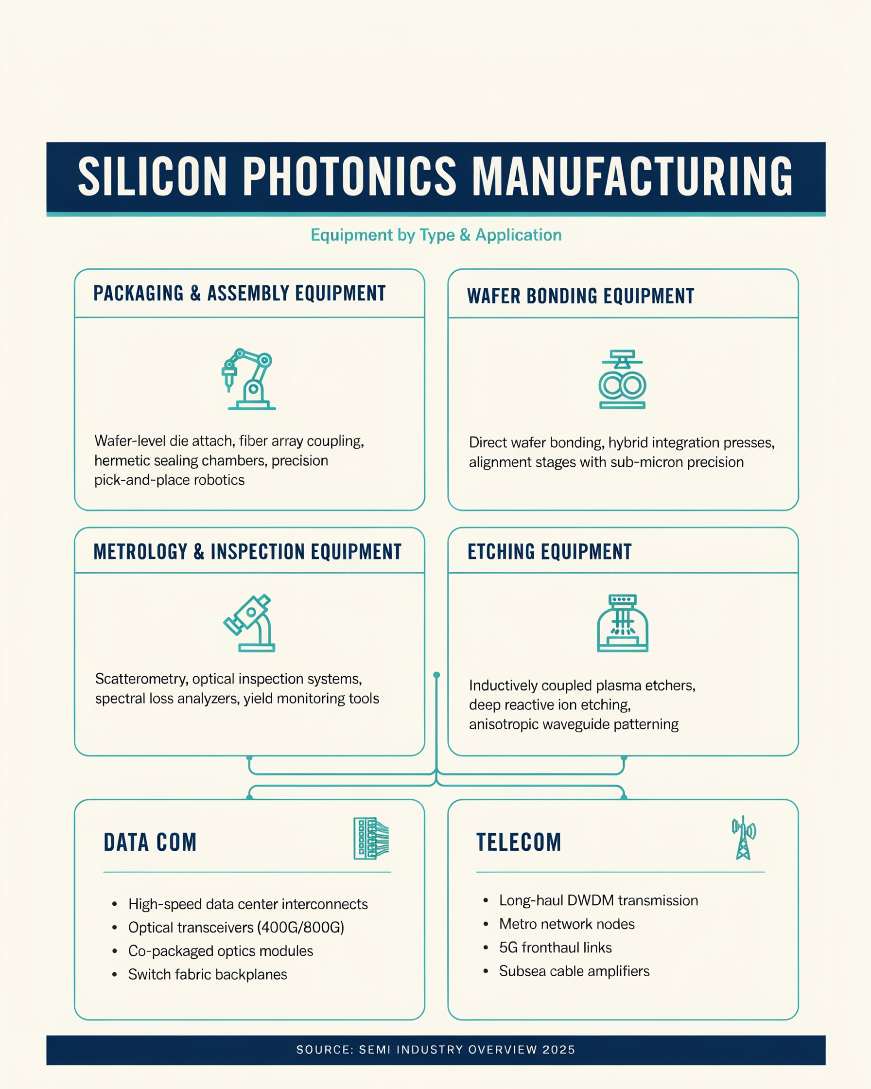
Manufacturing Challenges Encourage Equipment Innovation
Despite growing investments, advanced semiconductor packaging for silicon photonics faces challenges related to equipment costs, process complexity, production scalability, and reliability. Manufacturers must maintain precise optical alignment while managing thermal and mechanical constraints within increasingly compact packages. Differences between semiconductor and photonic manufacturing processes can also complicate integration.
Equipment suppliers are addressing these challenges through improved automation, advanced process monitoring, and flexible manufacturing platforms. Data analytics and AI-based monitoring can help identify process variations, optimize equipment performance, and reduce unplanned downtime. Collaboration among semiconductor manufacturers, foundries, OSAT providers, and photonic technology developers is also supporting improvements in packaging processes.
Future Outlook for Silicon Photonics Manufacturing Growth
Advanced semiconductor packaging investments are expected to remain an important factor supporting silicon photonics manufacturing growth. Increasing demand for AI computing, data center connectivity, high-speed telecommunications, and optical networking will encourage further development of advanced integration technologies.
Future investments are likely to emphasize co-packaged optics, heterogeneous integration, wafer-level packaging, automated optical alignment, and high-precision testing. Equipment suppliers capable of delivering scalable and reliable manufacturing solutions will be well positioned to benefit from these developments. As silicon photonics becomes increasingly important to next-generation digital infrastructure, advanced semiconductor packaging will play a critical role in improving production efficiency, device performance, and commercial adoption.