
The global Hybrid Bonding Technology Market is witnessing significant growth as semiconductor manufacturers increasingly adopt advanced packaging technologies to meet the rising demand for high-performance, energy-efficient, and compact electronic devices. The rapid expansion of artificial intelligence (AI), high-performance computing (HPC), high-bandwidth memory (HBM), and next-generation semiconductor architectures is accelerating the adoption of hybrid bonding technology across the global semiconductor industry.
According to MarketsandMarkets, the global hybrid bonding market is projected to grow from USD 0.38 billion in 2026 to USD 2.45 billion by 2033, registering a compound annual growth rate (CAGR) of 30.3% during the forecast period. The growing need for high-density interconnections, improved data transfer speeds, reduced power consumption, and advanced three-dimensional (3D) chip integration is expected to create substantial growth opportunities for market participants.
Rising Adoption of Advanced Semiconductor Packaging Technologies
The increasing complexity of semiconductor devices is driving manufacturers to explore innovative packaging solutions capable of delivering higher performance within smaller physical footprints. Traditional packaging technologies are facing limitations in supporting the growing requirements of modern computing systems, particularly in terms of interconnect density, bandwidth, and energy efficiency.
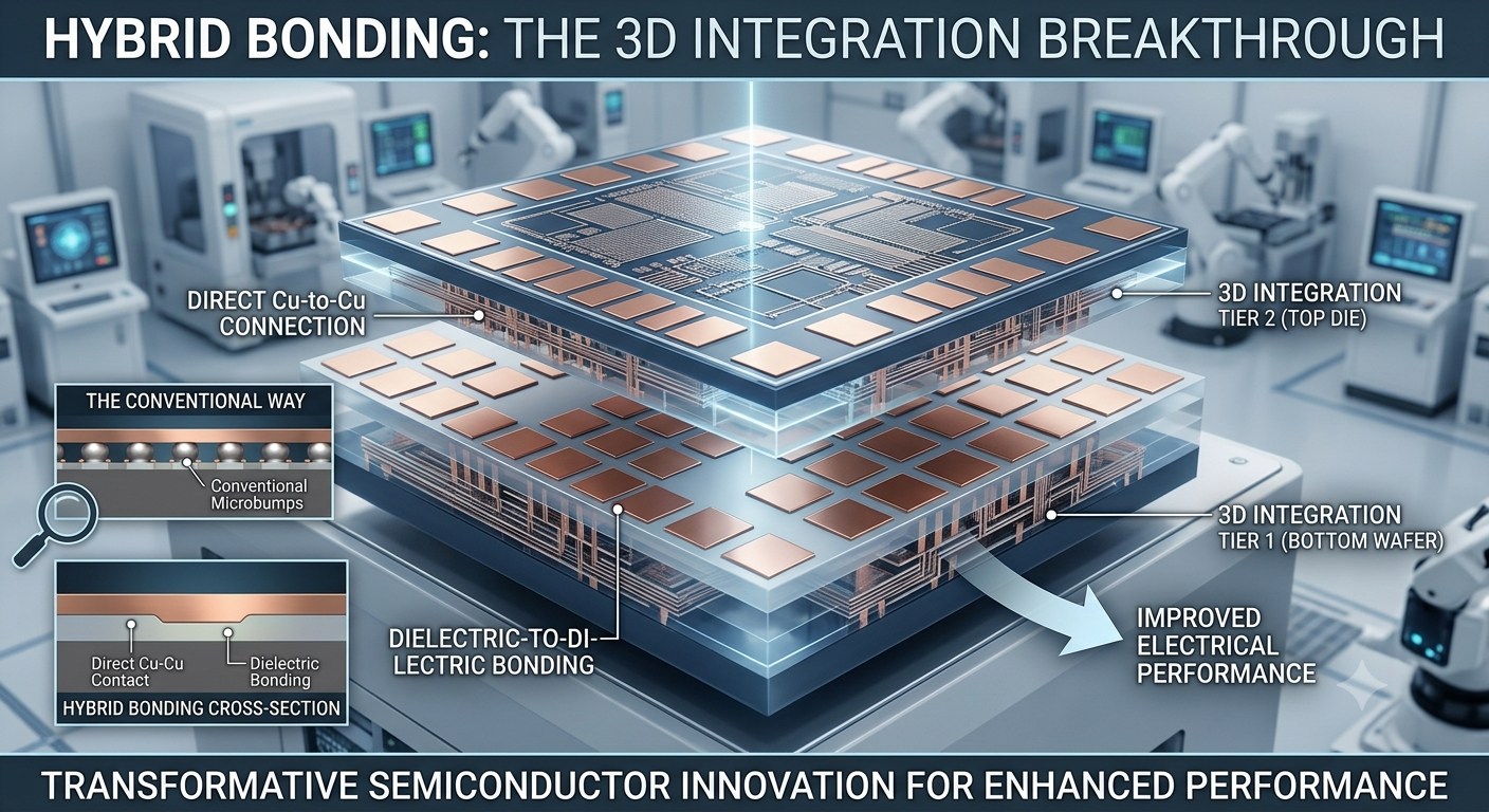
Hybrid bonding technology addresses these limitations by enabling direct bonding between copper interconnects and dielectric surfaces without relying on conventional solder microbumps. This approach facilitates ultra-fine-pitch interconnections, shorter electrical pathways, improved signal transmission, and higher integration density.
The technology is gaining traction in 3D-stacked integrated circuits, chiplet-based architectures, advanced memory devices, CMOS image sensors, and heterogeneous integration applications. As semiconductor manufacturers continue to develop increasingly sophisticated chip architectures, hybrid bonding is emerging as an important technology for next-generation semiconductor packaging.
Download PDF Brochure @ https://www.marketsandmarkets.com/pdfdownloadNew.asp?id=2641237
Growing AI and High-Performance Computing Demand Accelerates Market Growth
The rapid development of artificial intelligence, machine learning, cloud computing, and data center infrastructure is creating substantial demand for advanced semiconductor solutions. AI accelerators and high-performance processors require high-speed communication between logic and memory components to handle increasingly complex workloads.
Hybrid bonding enables high-density vertical interconnections that support faster data transfer, lower latency, and improved power efficiency. These capabilities make the technology particularly suitable for AI processors, graphics processing units (GPUs), high-bandwidth memory, and advanced computing systems.
Furthermore, the increasing adoption of generative AI and large-scale data processing applications is encouraging semiconductor manufacturers to invest in advanced packaging technologies. Hybrid bonding is expected to play an increasingly important role in enabling compact, high-performance semiconductor architectures.
Die-to-Wafer Bonding Segment Creates Significant Growth Opportunities
Based on packaging architecture, the die-to-wafer (D2W) segment is expected to register strong growth during the forecast period. According to MarketsandMarkets, this segment is projected to grow at a CAGR of 44.2%.
Die-to-wafer bonding enables individual semiconductor dies to be integrated onto a target wafer, offering flexibility in combining different chip technologies and functionalities. The approach supports heterogeneous integration while allowing manufacturers to select known-good dies, potentially improving manufacturing yields and reducing production costs.
Increasing applications in AI accelerators, high-bandwidth memory, chiplet architectures, and high-performance computing are strengthening demand for die-to-wafer hybrid bonding solutions. Its ability to support advanced chip integration and high-density interconnections is expected to contribute significantly to market expansion.
Asia Pacific Maintains a Strong Position in the Hybrid Bonding Market
Asia Pacific represents a major regional market for hybrid bonding technology, supported by its established semiconductor manufacturing ecosystem and growing investments in advanced packaging capabilities. According to MarketsandMarkets, the region accounted for approximately 52.3% of the global hybrid bonding market in 2025.
Countries such as China, Japan, South Korea, and Taiwan are playing important roles in semiconductor manufacturing, memory production, wafer fabrication, and advanced packaging development.
The presence of major semiconductor manufacturers and technology suppliers, combined with increasing investments in high-bandwidth memory, 3D integrated circuits, and AI-focused semiconductor solutions, is supporting regional market growth.
Additionally, the growing demand for advanced consumer electronics, automotive semiconductors, and high-performance computing devices is expected to strengthen the adoption of hybrid bonding technology across the region.
Technological Advancements and Strategic Collaborations Shape the Competitive Landscape
Leading semiconductor equipment manufacturers and technology developers are focusing on product innovation, strategic partnerships, and advanced bonding solutions to strengthen their market positions.
Key companies operating in the hybrid bonding market include BE Semiconductor Industries (Besi), Tokyo Electron Limited, EV Group (EVG), Piotech, Inc., ASMPT, Applied Materials, Inc., SUSS MicroTec SE, Kulicke & Soffa Industries, Inc., and SHIBAURA MECHATRONICS CORPORATION.
Companies are increasingly investing in precision alignment, surface preparation, wafer cleaning, metrology, and copper-to-copper bonding technologies to improve manufacturing accuracy, production efficiency, and bonding reliability.
Recent industry developments further demonstrate the growing importance of hybrid bonding technology. In October 2026, Applied Materials and Besi expanded their strategic partnership, with Besi joining Applied Materials’ EPIC Center as an Innovation Partner. The collaboration focuses on next-generation hybrid bonding, 3D integrated circuit scaling, logic and memory integration, and advanced packaging solutions for AI infrastructure.
Similarly, in June 2026, SUSS MicroTec introduced its XBC300 Gen2 SP surface-preparation cluster for advanced hybrid bonding applications. The platform supports wafer-to-wafer and die-to-wafer bonding through integrated cleaning, plasma activation, void detection, and metrology capabilities.
These developments highlight the industry’s increasing focus on improving bonding precision, manufacturing scalability, and production yields.
Market Challenges and Emerging Opportunities
Despite its strong growth potential, the hybrid bonding market faces several challenges that could influence adoption across the semiconductor manufacturing industry.
High initial capital investment remains a significant barrier, as hybrid bonding requires specialized equipment for wafer bonding, surface preparation, cleaning, precision alignment, and process monitoring. These requirements can increase manufacturing costs and create challenges for smaller semiconductor manufacturers.
Maintaining extremely clean surfaces and achieving precise wafer alignment are also critical to ensuring reliable bonding performance. Even minor contamination or alignment defects can affect manufacturing yields and production efficiency.
However, growing investments in AI and machine learning accelerators, advanced memory technologies, and heterogeneous integration are creating new opportunities for market participants. The increasing deployment of hybrid bonding in CMOS image sensors, augmented reality (AR), virtual reality (VR), and next-generation automotive electronics is also expected to support market expansion.
Future Outlook
The global hybrid bonding technology market is expected to experience substantial growth as semiconductor manufacturers increasingly transition toward advanced packaging, 3D integration, and chiplet-based architectures. Rising demand for AI processors, high-bandwidth memory, high-performance computing, and energy-efficient semiconductor devices will remain important factors supporting market expansion.
Continuous advancements in wafer-to-wafer and die-to-wafer bonding, copper-to-copper interconnections, surface preparation, and precision alignment are expected to improve manufacturing capabilities and broaden commercial adoption.
With increasing investments from semiconductor manufacturers, equipment suppliers, and technology developers, hybrid bonding is positioned to become an important enabler of next-generation semiconductor innovation. The market is therefore expected to offer significant opportunities for companies developing advanced bonding equipment, materials, and integrated semiconductor packaging solutions.
Frequently Asked Questions (FAQs)
1. What is the global hybrid bonding technology market size?
The global hybrid bonding market is projected to grow from USD 0.38 billion in 2026 to USD 2.45 billion by 2033, according to MarketsandMarkets.
2. What is the expected CAGR of the hybrid bonding market?
The market is expected to register a CAGR of 30.3% during the forecast period from 2026 to 2033.
3. What are the major factors driving the growth of the hybrid bonding market?
Key growth drivers include increasing demand for artificial intelligence (AI) processors, high-performance computing (HPC), high-bandwidth memory (HBM), 3D integrated circuits, and advanced semiconductor packaging technologies.
4. What is hybrid bonding technology?
Hybrid bonding is an advanced semiconductor packaging technology that directly connects copper interconnects and dielectric surfaces between semiconductor dies or wafers. It enables high-density interconnections, improved electrical performance, and efficient 3D chip integration.
5. Which packaging architecture is expected to grow fastest in the hybrid bonding market?
The die-to-wafer (D2W) segment is expected to register the highest growth, with a projected CAGR of 44.2% during 2026–2033.
6. Which region dominates the hybrid bonding market?
Asia Pacific held approximately 52.3% of the global hybrid bonding market in 2025, supported by its strong semiconductor manufacturing ecosystem and investments in advanced packaging technologies.