The Hybrid Bonding Market is experiencing strong growth momentum as the semiconductor industry accelerates its transition toward advanced packaging technologies. Hybrid bonding has emerged as a critical innovation enabling higher interconnect density, improved electrical performance, and enhanced power efficiency in next-generation semiconductor devices.
As demand for artificial intelligence (AI), high-performance computing (HPC), 5G/6G infrastructure, and advanced consumer electronics continues to rise, semiconductor manufacturers are increasingly investing in hybrid bonding solutions to overcome scaling limitations of traditional packaging methods. The Hybrid Bonding Market growth is being driven by rising capital investments, technological advancements, and the need for ultra-miniaturized, high-performance chips.
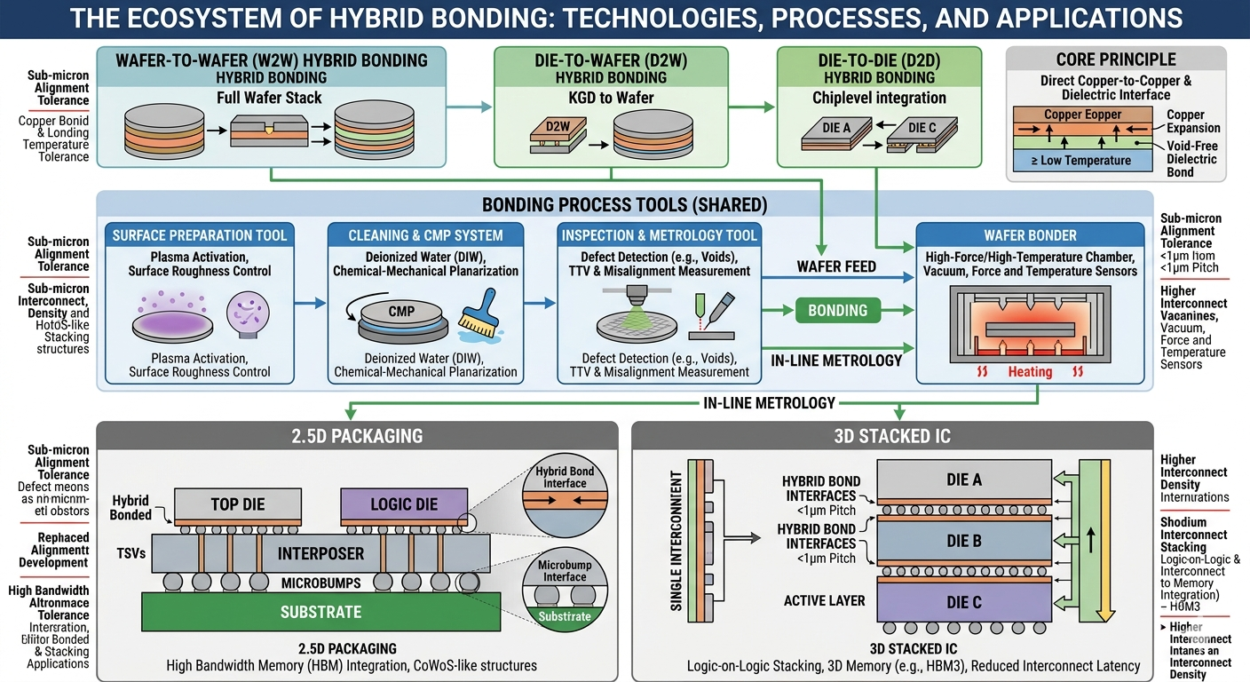
Understanding Hybrid Bonding Technology
Hybrid bonding is an advanced semiconductor packaging technique that directly connects copper-to-copper and dielectric-to-dielectric layers without using solder bumps. This enables extremely fine pitch interconnections, improved signal integrity, and higher bandwidth performance.
Unlike traditional flip-chip or wire bonding methods, hybrid bonding allows:
- Ultra-high interconnect density
- Lower electrical resistance
- Improved thermal performance
- Enhanced chip-to-chip communication
- Greater scalability for 2.5D and 3D IC architectures
These advantages are making hybrid bonding a foundational technology in advanced semiconductor manufacturing, significantly contributing to Hybrid Bonding Market growth.
Key Drivers of Hybrid Bonding Market Growth
1. Rising Semiconductor Investments
One of the primary factors driving Hybrid Bonding Market growth is the surge in global semiconductor investments. Governments and private companies are heavily investing in semiconductor fabrication plants (fabs), advanced packaging facilities, and R&D initiatives.
Major semiconductor players are allocating billions of dollars to expand production capacity and develop next-generation packaging technologies. Hybrid bonding is increasingly seen as essential for achieving performance gains in advanced chips used in AI accelerators, data centers, and mobile devices.
2. Growth of Artificial Intelligence and HPC Applications
The rapid expansion of AI and high-performance computing is significantly boosting demand for advanced semiconductor packaging solutions. AI workloads require massive data processing capabilities, which depend on high-bandwidth memory and efficient chip integration.
Hybrid bonding enables closer integration of logic and memory chips, reducing latency and improving performance. This makes it a key enabler of AI-driven systems, thereby accelerating Hybrid Bonding Market growth.
3. Transition to Advanced Packaging Technologies
As Moore’s Law slows down, semiconductor companies are shifting focus from transistor scaling to advanced packaging technologies. Hybrid bonding is at the forefront of this transition, enabling:
- 3D integrated circuits (3D ICs)
- Chiplet-based architectures
- High-bandwidth memory integration
This technological shift is a major contributor to the expansion of the Hybrid Bonding Market.
Download PDF Brochure @ https://www.marketsandmarkets.com/pdfdownloadNew.asp?id=2641237
Applications Driving Market Expansion
AI and Data Centers
AI processors and data center chips require extremely high bandwidth and energy efficiency. Hybrid bonding allows tighter integration between compute and memory units, making it ideal for AI accelerators and cloud infrastructure.
Consumer Electronics
Smartphones, tablets, and wearable devices are becoming increasingly compact and powerful. Hybrid bonding supports miniaturization while enhancing performance, driving adoption in consumer electronics manufacturing.
Automotive Electronics
The automotive sector is rapidly adopting advanced semiconductor technologies for autonomous driving, electric vehicles (EVs), and ADAS systems. Hybrid bonding ensures high reliability and performance under demanding conditions.
Telecommunications (5G/6G)
Hybrid bonding supports high-speed signal processing required for next-generation wireless networks, making it critical for 5G and future 6G infrastructure.
Investment Trends in the Hybrid Bonding Market
The Hybrid Bonding Market growth is strongly supported by increasing investments across the semiconductor ecosystem.
Capital Expenditure Expansion
Leading semiconductor companies are significantly increasing capital expenditure (CAPEX) to develop advanced packaging capabilities. Hybrid bonding equipment and materials are receiving higher investment priority due to their strategic importance.
Equipment Manufacturer Innovation
Equipment providers are investing in new bonding systems that offer higher precision, scalability, and yield improvement. These innovations are essential for commercializing hybrid bonding at scale.
Strategic Partnerships and Collaborations
The market is witnessing a rise in partnerships between semiconductor fabs, equipment manufacturers, and research institutions. These collaborations aim to accelerate hybrid bonding adoption and reduce production complexity.
Challenges in the Hybrid Bonding Market
Despite strong growth, several challenges impact the Hybrid Bonding Market growth:
- High equipment and process costs
- Complex manufacturing requirements
- Yield optimization challenges at scale
- Limited standardization across the industry
However, ongoing R&D efforts and process improvements are expected to address these limitations over time.
Regional Outlook
Asia Pacific
Asia Pacific dominates the Hybrid Bonding Market due to strong semiconductor manufacturing ecosystems in countries such as Taiwan, South Korea, China, and Japan. These regions host leading foundries and packaging companies investing heavily in advanced technologies.
North America
North America is witnessing strong growth driven by AI chip development, data center expansion, and government initiatives supporting domestic semiconductor manufacturing.
Europe
Europe is focusing on automotive semiconductors and industrial applications, contributing steadily to market growth.
Future Outlook
The future of the Hybrid Bonding Market growth is closely tied to advancements in semiconductor scaling, chiplet architectures, and AI-driven computing systems. As demand for higher performance and energy efficiency continues to rise, hybrid bonding will become a mainstream technology in advanced semiconductor packaging.
By enabling ultra-dense interconnects and improved system integration, hybrid bonding is expected to play a central role in shaping the next generation of computing platforms.
The Hybrid Bonding Market growth is gaining strong momentum due to rising semiconductor investments, rapid expansion of AI and HPC applications, and the global shift toward advanced packaging technologies. Despite manufacturing challenges, continuous innovation and strategic investments are driving widespread adoption.
As the semiconductor industry evolves, hybrid bonding is set to become a cornerstone technology, enabling faster, smaller, and more efficient electronic systems across multiple industries
FAQs