The AI impact analysis on the Extreme Ultraviolet Lithography (EUVL) industry reveals how artificial intelligence is transforming the entire EUV ecosystem, particularly across its core components — Light Sources, Optics, Masks, EUV Metrology, EUV Sensors, and Subassemblies. These elements form the backbone of EUVL systems, and each is being enhanced by AI to support greater precision, efficiency, and reliability in semiconductor manufacturing.
Starting with Light Sources, which generate the 13.5 nm wavelength needed for EUV lithography, AI plays a crucial role in optimizing plasma generation and maintaining beam stability. These light sources are notoriously difficult to control, requiring extreme precision in power, gas flow, and thermal management. AI algorithms analyze real-time sensor data to dynamically adjust source parameters, ensuring consistent intensity and minimizing downtime. Through predictive maintenance models, AI can also forecast potential failures in the source module, helping to avoid unexpected outages that can disrupt chip production schedules.
In Optics, which include complex multilayer mirrors used to guide and focus EUV light, AI helps monitor degradation and alignment issues that affect reflectivity and imaging quality. Given that even atomic-level imperfections can compromise optical performance, AI-powered systems analyze optical path data and environmental variables to calibrate focus and correct distortions in real time. This allows for improved image fidelity and higher patterning accuracy, which is critical as semiconductor nodes shrink below 5nm.
Download PDF Brochure @ https://www.marketsandmarkets.com/pdfdownloadNew.asp?id=241564826
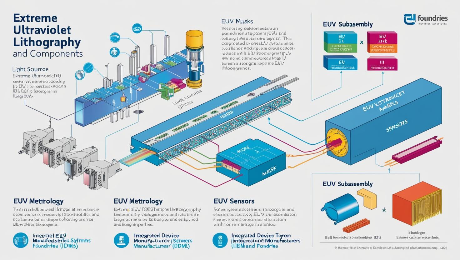
When it comes to EUV Masks, AI assists in inspecting and optimizing mask design and defect repair. Due to the opaque nature of EUV masks and the absence of pellicles in some applications, contamination or defects can directly impact the wafer yield. AI-based image recognition and pattern analysis tools can detect sub-nanometer defects in mask layers, differentiate between critical and non-critical anomalies, and guide automated repair systems. Additionally, AI aids in computational lithography, where it helps simulate how mask patterns will print under varying process conditions — leading to more robust mask layouts and fewer print errors.
Extreme Ultraviolet (EUV) Lithography Industry Growth
The EUV lithography Industry is expected to reach USD 22.69 billion by 2029 from USD 12.18 billion in 2024, at a CAGR of 13.2% during the 2024-2029 period
EUV Metrology, essential for measuring line widths, critical dimensions, and overlay accuracy, is another area where AI is making major strides. AI-enhanced metrology tools analyze vast quantities of image and process data to identify trends, detect anomalies, and ensure pattern consistency across wafers. These tools reduce the need for manual inspection and improve measurement throughput without compromising accuracy. Furthermore, AI models are used to predict metrology drift and recalibrate tools automatically, maintaining system precision over extended operation cycles.
The role of EUV Sensors — which monitor system variables like temperature, pressure, alignment, and beam characteristics — has been significantly elevated with AI. Traditional sensors generate immense data streams that were once underutilized, but now, AI systems can process and interpret this data in real-time. These intelligent systems identify fluctuations that may indicate process instability or early signs of equipment wear. By enabling closed-loop control and real-time process optimization, AI ensures better stability and repeatability in EUV exposure.
Finally, in EUV Subassembly components, which include stages, actuators, cooling systems, and support infrastructure, AI contributes to system diagnostics, operational efficiency, and lifecycle management. AI algorithms monitor subassembly performance, detect deviations from standard operation, and recommend preventive interventions. By optimizing the movement and coordination of subcomponents — such as wafer handling systems and lens positioning — AI enhances the overall productivity and accuracy of EUV lithography tools.
In summary, the integration of artificial intelligence across every major component of the EUVL system is revolutionizing semiconductor manufacturing. From intelligent light source management and adaptive optics to predictive sensor analytics and AI-guided metrology, each part of the EUV process is becoming more autonomous, resilient, and efficient. This AI-driven transformation ensures not only improved chip yield and reduced manufacturing defects but also faster innovation cycles in an industry where every nanometer counts.