As the semiconductor industry pushes past the limits of traditional photolithography, Extreme Ultraviolet Lithography (EUVL) has emerged as the most critical enabler of advanced node manufacturing. Capable of producing chips at 7nm, 5nm, and beyond, EUVL is redefining what’s possible in transistor scaling, power efficiency, and device performance.
The EUVL market is no longer a future bet—it is the present-day backbone of high-performance chip fabrication, with growing adoption among foundries, integrated device manufacturers (IDMs), and equipment suppliers across the globe.
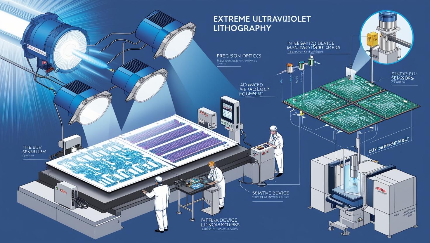
Why EUVL Matters: Precision at the Atomic Scale
EUVL uses light at a wavelength of just 13.5 nanometers, far shorter than traditional deep ultraviolet (DUV) lithography, which operates around 193nm. This enables manufacturers to etch smaller, more complex features onto wafers with fewer patterning steps—drastically improving throughput, yield, and power efficiency.
With the demand for smaller, faster, and more energy-efficient chips across AI, 5G, HPC, and consumer electronics, EUVL has become essential to maintaining the pace of innovation defined by Moore’s Law.
Key Market Trends Driving EUVL Growth
1. AI and HPC Driving Advanced Node Demand
As workloads for artificial intelligence, machine learning, and high-performance computing intensify, chipmakers require fabrication technologies that support ultra-dense transistor architectures. EUVL’s ability to support advanced nodes (5nm, 3nm, and 2nm) makes it indispensable in the production of leading-edge processors.
2. Foundry Investments in EUV Capacity
Leading foundries such as TSMC, Samsung, and Intel have aggressively invested in EUVL tools to maintain their competitiveness. TSMC, in particular, has embedded EUV into its 5nm and 3nm processes and is working toward 2nm and below. These expansions are fueling demand for EUV scanners, photoresists, pellicles, and metrology tools.
Download PDF Brochure @ https://www.marketsandmarkets.com/pdfdownloadNew.asp?id=241564826
3. Equipment Supply Chain Consolidation
Dutch company ASML remains the sole provider of commercial EUV scanners, giving it a dominant position in the lithography equipment market. Its highly specialized EUV tools, which can cost over $150 million each, are at the heart of every advanced semiconductor fab today.
Meanwhile, companies like Zeiss (optics), Trumpf (light sources), and Carl Zeiss SMT are key suppliers within the EUV ecosystem, contributing to a highly consolidated but critically interdependent supply chain.
4. Shift Toward High-NA EUV
The next frontier in lithography is High-NA (Numerical Aperture) EUV, which promises even greater resolution and smaller feature sizes. ASML plans to ship its first High-NA EUV systems to early partners such as Intel and imec, opening doors for sub-2nm manufacturing by 2026–2027.
Leading Companies in the EUVL Market
-
ASML (Netherlands) – Dominates the EUV scanner market; central to the global lithography supply chain.
-
TSMC (Taiwan) – Largest EUV adopter among foundries, producing at 5nm and 3nm for clients like Apple and AMD.
-
Samsung Electronics (South Korea) – Competing with TSMC on EUV-based production for mobile and HPC chips.
-
Intel (USA) – Investing in EUV and High-NA to regain leadership in advanced process nodes.
-
Lam Research, KLA, Applied Materials (USA) – Provide essential metrology, deposition, and etch solutions that support EUV workflows.
Challenges in EUVL Adoption
Despite its transformative capabilities, EUVL is not without challenges:
-
High cost of equipment and maintenance
-
Technical complexity in optics, mirrors, and light source generation
-
Low supply chain redundancy (limited suppliers for critical components)
-
Resist and mask defects that affect production yields
-
Extreme infrastructure requirements for vibration and contamination control
These challenges mean EUVL remains concentrated among a few high-capital firms, making it less accessible to mid-tier and emerging players.
What Comes Next in EUVL and Semiconductor Innovation?
1. High-NA EUV Deployment
The rollout of High-NA EUV systems will mark the next era of atomic-scale manufacturing. By increasing resolution, these systems allow for even denser and more energy-efficient chips—critical for future AI models, quantum computing, and immersive technologies.
2. Materials Innovation
New photoresists, pellicles, and optical coatings are in development to increase EUV throughput and reduce defects. Collaboration between fabs, academia, and material science companies will be essential.
3. EUV Integration Across More Nodes
While EUV was first adopted at 7nm and 5nm, it’s now being integrated into mainstream nodes (e.g., 10nm and 12nm) to optimize performance and extend legacy technology.
4. Localization and Supply Chain Diversification
To reduce geopolitical risk, countries like the U.S., Japan, South Korea, and members of the EU are investing in domestic EUV manufacturing capabilities and component supply to ensure resilience in future chip production.
Conclusion: EUVL Is the Heart of Next-Gen Semiconductors
Extreme Ultraviolet Lithography is not just an innovation—it’s the foundation for the future of semiconductors. As demand for smaller, smarter, and more powerful chips grows across industries, the EUVL market is set to expand rapidly over the next decade.
With strong market drivers, a highly specialized ecosystem, and next-gen technologies like High-NA on the horizon, EUVL will remain central to semiconductor leadership and national competitiveness worldwide.
FAQ: Extreme Ultraviolet Lithography (EUVL) Market
1. What is Extreme Ultraviolet Lithography (EUVL)?
EUVL is an advanced photolithography technology that uses 13.5 nm wavelength light to etch extremely fine patterns on semiconductor wafers. It enables the production of smaller, faster, and more power-efficient chips used in advanced computing, smartphones, and AI applications.
2. Why is EUVL important for semiconductor manufacturing?
EUVL is critical for manufacturing chips at advanced nodes like 7nm, 5nm, 3nm, and below, where traditional lithography techniques (DUV) become less efficient and more complex. EUVL simplifies the manufacturing process while improving performance, yield, and cost-effectiveness in the long term.
3. Who are the major players in the EUVL market?
- ASML (Netherlands): The only supplier of EUV scanners globally.
- TSMC (Taiwan): The largest adopter of EUV for advanced chips.
- Samsung (South Korea): Aggressively investing in EUV for logic and memory chips.
- Intel (USA): Expanding EUV capabilities for advanced process nodes.
- KLA, Lam Research, Applied Materials: Provide supporting metrology and etch solutions.
4. What industries are driving EUVL demand?
- EUVL is primarily driven by:
- Semiconductor foundries and IDMs
- Artificial Intelligence (AI) and High-Performance Computing (HPC)
- 5G infrastructure
- Consumer electronics
- Automotive (ADAS and EV chips)